Disco
DAD641
Provisional entry — research in progress
This page was generated automatically from cited public sources and hasn't completed the full research pass yet. Every specification shown carries its source; more detail is added as research completes.
The Disco DAD641 is a dicing saw used for wafer dicing. The Disco DAD641 can dice wafers into small substrates, such as 5×5 mm2 pieces.[1]
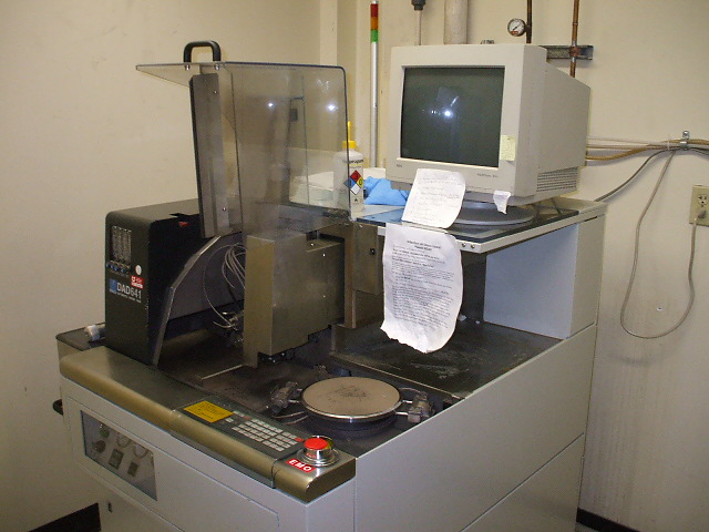
Plate 01DAD641 alignment 1
NTCRaymondWatch on YouTubePlate 02DAD641 wafer 2
NTCRaymondWatch on YouTube
What it is
General reference — not yet source-verifiedA dicing saw is a wafer singulation tool used to cut processed substrates into individual dies or chips. Dicing saws are part of backend microfabrication and packaging work, where patterned wafers or other substrates are separated after earlier device-forming steps are complete.
What do the numbers mean?
Wafer handling2
Configuration & options5
What replaced it?
Related models
- siblingDisco DAD3220— Listed on the same equipment page under packaging equipment.source[3]
Where are the manuals?
Generated from public-source data on file. Enter your email to access — nothing is published; details are routed privately.
Not publicly documented
Field notes
No research found yet — worked with this tool? Share what you know.
Frequently asked questions
What kind of tool is the Disco DAD641?
The Disco DAD641 is a dicing saw.[3]
Not publicly documented
The following facts about the DAD641 are absent from this record as of this revision. First-hand knowledge or a citation closes a gap; every submission is reviewed before publication.
No publicly documented production dates or lifecycle milestones (introduction, end of production, EOL) for the DAD641 are on record.
Answerable by: OEM historical records or a trade-press announcement
No publicly documented variants, configuration options, or revision breakpoints of the DAD641 are on record.
Answerable by: an OEM product catalog or an engineer who ordered or specified the tool
The control-system platform and OS era of the DAD641 are not on record.
Answerable by: an engineer who operated it or OEM installation records
No publicly documented failure modes or field errata for the DAD641 are on record.
Answerable by: a field service engineer, process engineer, or maintenance technician
The process node or technology generation of the DAD641 is not on record.
Answerable by: an OEM datasheet or a fab qualification report
No research found yet — worked with this tool? Share what you know.
Sources & citations
Sources (4)Every fact above is drawn from these public sources
- [1]arxiv.org — arxiv.orgarxiv.org
- [2]nanofab.utah.edu — nanofab.utah.edunanofab.utah.edu
- [3]nanofab.utah.edu — nanofab.utah.edunanofab.utah.edu
- [4]nanofab.utah.edu — nanofab.utah.edunanofab.utah.edu
Last updated Oct 20, 2026.
Compare with similar tools
View all →
The Lapmaster Model 15 is a bench-mounted unit with a rigid, lightweight, cast aluminum base, of the 'ring lapper' configuration, enabling high standards of flatness and surface finish.

The Blanchard 18 D Surface is a surface grinder used in Dicing & Grinding applications.

The Blanchard 20 36 Surface is a surface grinder used in dicing and grinding applications.
