Leica
DM8000
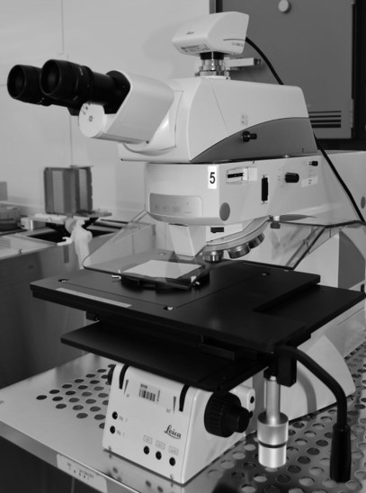
Plate 01Leica DM8000 M Videos Leica Microsystems
Công ty TNHH Sao Đỏ Việt NamWatch on YouTubePlate 02Leica DM8000 M Videos Leica Microsystems 2
Công ty TNHH Sao Đỏ Việt NamWatch on YouTubePlate 03Leica DM8000 M Videos Leica Microsystems 3
Công ty TNHH Sao Đỏ Việt NamWatch on YouTubePlate 04Promicron AOI wafer inspection, diced wafer on bluetape filmframe, Deep Learning AOI, Leica DM8000
Firma Promicron GmbHWatch on YouTubePlate 05Leica DM8000 M Videos Leica Microsystems 1
Công ty TNHH Sao Đỏ Việt NamWatch on YouTube
What it is
The Leica DM8000 M is an optical inspection system used for the examination and process control of wafers, LCD displays, and other industrial samples. The Leica DM8000 M and the Leica DM12000 M are a line of high-throughput inspection systems developed by Leica Microsystems for the semiconductor industry. The Leica DM8000 M incorporates full LED incident light illumination and supports viewing techniques including brightfield, darkfield, differential interference contrast (DIC), qualitative polarization, oblique illumination, UV, and OUV (oblique UV). The system features a motorized objective nosepiece with a 6-position design and is built around Leica HC optics corrected to infinity.[2][5]
How it works
The Leica DM8000 M operates as an upright microscope with a reflected light illumination path based on full LED technology. The LED illumination is integrated into the stand to optimize airflow and minimize heat radiation, which is important for cleanroom environments. The microscope uses a motorized objective nosepiece that is encapsulated for cleanroom compatibility and includes a mechanical and electronic focus stop to protect samples from damage.[2][3]
The microscope features an integrated contrast manager and illumination manager that automatically adjust parameters when switching between contrast modes. The OUV (oblique UV) mode combines oblique illumination with UV light to provide enhanced resolution and three-dimensional sample visualization. The motorized stage options include travel ranges of 202 x 202 mm for 8-inch wafer inspection, with both manual and motorized versions available. Control is provided via the Leica SmartMove device for x, y, and z positioning, or the Leica STP6000 stage controller.[2][3]
Where it fits in the process flow
The Leica DM8000 M can be upgraded to an inspection or review system by adding a wafer loader, vacuum wafer chucks, and inspection or film thickness measurement software. The system supports cleanliness analysis of mechanical parts through filter analysis, and is applicable to the inspection of LCDs and TFTs. The LED illumination contributes to a cleaner cleanroom environment by optimizing airflow and eliminating the need for lamp changes.[2]
Applications
The Leica DM8000 M can perform cleanliness analysis of mechanical parts via filter analysis. The system is also suitable for materials science applications such as the inspection of polished metal sections, composites, and minerals. The macro mode facilitates rapid scanning of large components for macro defects, while the micro mode allows detailed inspection using brightfield, darkfield, or DIC contrast.[2][3]
- inspection
- optical microscopy
- measurements
- overlay annotations
What do the numbers mean?
Power & electrical1
Optics & imaging7
- Viewing tube
- Trinocular Ergotube with upright and unreversed image; beam splitting 100/0 and 0/100 (eyepiece/camera)[2]
- Illumination
- Full LED incident light illumination; viewing techniques: Brightfield, darkfield, DIC, qualitative POL, oblique illumination, UV, OUV. Also full LED transmitted light illumination; BF, POL.[2]
- Objective nosepiece
- Motorized, 6-position for BD objectives with M32 thread, absolutely encoded[3]
- Ambient temperature range
- 15–35 °C (without IR illumination); 15–28 °C (with IR illumination)[3]
Performance1
Control & software1
Dimensions & facilities2
- Focus
- Manual: heavy-duty 2-stage, coarse and fine, 35 mm travel range, height-adjustable knobs. Motorized: 2-stage with 35 mm travel range, high reproducibility, parfocality compensation.[2]
Configuration & options6
- Imaging modes
- Bright Field (BF), Dark Field (DF), and Differential Interference Contrast (DIC)[1]
- Stage (manual)
- 8-inch manual inspection stage; travel range 202 mm × 202 mm in reflected and transmitted light; integrated rapid adjustment[2]
- Stage (motorized)
- 8-inch scanning stage; travel range 200 mm × 200 mm in reflected and transmitted light; 4 mm pitch spindle; max speed 240 mm/s[3]
What replaced it?
Related models
- siblingNikon Optiphot 200— Listed on the same microscopes pagesource[4]
What does it need to run?
Site utility requirements, footprint, and infrastructure needed to install and operate this tool. Sourced from public records.
- Power supply100–120/220–240 V AC, 50/60 Hz[2]
Where are the manuals?
Generated from public-source data on file. Enter your email to access — nothing is published; details are routed privately.
Not publicly documented
Field notes
No research found yet — worked with this tool? Share what you know.
Frequently asked questions
What is the maximum wafer size the Leica DM8000 M can inspect?
The Leica DM8000 M is designed for inspection of wafers up to 200 mm (8 inches) in diameter.[6]
What illumination source does the Leica DM8000 M use?
The Leica DM8000 M uses full LED incident light illumination that is integrated into the stand.[2]
What contrast techniques are available on the Leica DM8000 M?
The Leica DM8000 M supports brightfield, darkfield, DIC, qualitative POL, oblique illumination, UV, and OUV (oblique UV) viewing techniques.[2]
Does the Leica DM8000 M support macro imaging?
Yes, the Leica DM8000 M features a macro mode that captures an object field of up to 40 mm, providing approximately four times the field of view of conventional scanning objectives.[2]
What type of stage options are available for the Leica DM8000 M?
The Leica DM8000 M offers a manual inspection stage with 202 x 202 mm travel range and a motorized scanning stage with the same travel range, both for incident and transmitted light techniques.[2]
Not publicly documented
The following facts about the DM8000 are absent from this record as of this revision. First-hand knowledge or a citation closes a gap; every submission is reviewed before publication.
No publicly documented production dates or lifecycle milestones (introduction, end of production, EOL) for the DM8000 are on record.
Answerable by: OEM historical records or a trade-press announcement
No publicly documented variants, configuration options, or revision breakpoints of the DM8000 are on record.
Answerable by: an OEM product catalog or an engineer who ordered or specified the tool
The control-system platform and OS era of the DM8000 are not on record.
Answerable by: an engineer who operated it or OEM installation records
No publicly documented failure modes or field errata for the DM8000 are on record.
Answerable by: a field service engineer, process engineer, or maintenance technician
The process node or technology generation of the DM8000 is not on record.
Answerable by: an OEM datasheet or a fab qualification report
No research found yet — worked with this tool? Share what you know.
Sources & citations
Sources (6)Every fact above is drawn from these public sources
- [1]epfl.ch — epfl.chepfl.ch
- [2]downloads.leica-microsystems.com — downloads.leica-microsystems.comdownloads.leica-microsystems.com
- [3]opti-tech.ca — opti-tech.caopti-tech.ca
- [4]Microscopes at CMi ‒ Center of MicroNanoTechnology CMi ‐ EPFL — epfl.chepfl.ch
- [5]DM8000 M & DM12000 M Optical inspection systems | Products | Leica Microsystems — leica-microsystems.comleica-microsystems.com
- [6]Leica DM8000 M Microscope – I. Miller Microscopes — imillermicroscopes.comimillermicroscopes.com
Last updated Sep 3, 2026.
Compare with similar tools
View all →The KLA .204 PSL Wafer is an 8-inch NIST-traceable reference wafer compatible with Surfscan 6xy0 and Sp1 particle counters.
KLA .496 PSL Wafer is an 8-inch NIST traceable wafer stated to be capable on Surfscan 6xy0 and SP1.
The KLA .498 PSL Wafer is a NIST traceable reference wafer.
