PVA TePla
GigaBatch
The PVA TePla GigaBatch is a batch plasma stripper and surface cleaner that uses high-frequency microwave plasma at 2.45 GHz. The GigaBatch is designed for photoresist stripping, surface cleaning, and descuming before wet etching. The GigaBatch operates with oxygen gas and is available in two chamber variants: the GIGAbatch 360 and the GIGAbatch 380M.[1][2]
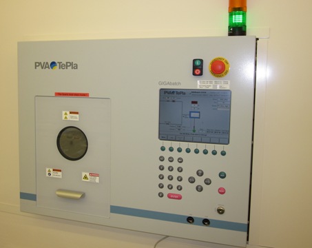
Plate 01PVATepla GIGABatch 360M O2 PLASMA power on DV
瀚柏科技 CO., LTDWatch on YouTubePlate 02穎強科技-PVA TePla 微波電漿清洗機 GIGAbatch 360 380P 介紹
Afen LiuWatch on YouTube
Wafer size
75 mm to 100 mm
Vacuum
Quartz primary vacuum chamber[1]
Performance
20% to 30% depending on process time[1]
Gas delivery
O2[1]
What it is
The PVA TePla GigaBatch is a microwave-frequency batch plasma stripper designed for photoresist stripping, surface cleaning, and descumming. The system operates at 2.45 GHz and is available in two chamber sizes: the GIGAbatch 360M with a 245 mm inner diameter quartz chamber, and the GIGAbatch 380M with a 300 mm inner diameter chamber. The GigaBatch can process wafers from 2 inches to 8 inches in diameter. The standard quartz holder accommodates 25 wafers, and higher throughput configurations support up to 75 wafers per run.[2][1]
How it works
The GigaBatch uses a quartz vacuum chamber. Plasma is generated by a microwave source at 2.45 GHz with power adjustable from 0 to 1000 W. Oxygen gas is introduced at flow rates up to 1000 ml/min. The process pressure is typically set at 0.5 mbar or 0.8 mbar for standard recipes. Wafers are loaded into a quartz boat that remains inside the chamber during operation.[2][1]
Where it fits in the process flow
The GigaBatch is used for photoresist stripping after lithography, wafer surface cleaning before subsequent processes, and descumming prior to wet etching.[1]
Applications
The GigaBatch is suitable for stripping positive and negative photoresists. Allowed substrate materials include silicon, glass, and Pyrex. Metals such as gold, silver, copper, chromium, and iron are not permitted in the chamber. Plastics can be processed with caution using a special holder and reduced power.[1]
- Photo resist stripping
- Wafer surface cleaning before subsequent processes
- Descumming before wet etching
Why won't it start?
Documented failure modes, common issues, and field considerations.
- Gold must not be loaded in the tool, even if covered and protected.
- Ag, Cu, Cr, and Fe are not welcome in the tool.
- Materials that deteriorate easily upon exposure to oxygen should not be processed in the machine.
What do the numbers mean?
Vacuum & pumping5
Wafer handling9
Gas & chemistry7
Performance1
Dimensions & facilities5
Configuration & options12
Vintage & configurations
What replaced it?
Related models
- siblingPVA TePla 300— Alternative for micro-electronic compatibilitysource[3]
What does it need to run?
Site utility requirements, footprint, and infrastructure needed to install and operate this tool. Sourced from public records.
- GasO2[1]
- Primary vacuum chamberQuartz primary vacuum chamber[1]
- Primary vacuum chamber dimensionsD int. 245 mm x Prof. 380 mm[1]
- Process gasO₂ (max flow 1000 ml/min)[1]
- Positive resist etch rate (high power)250 nm/min to 1.2 µm/min[1]
- Positive resist etch rate (low power)100 nm/min to 500 nm/min[1]
- Process gasO2 (max flow 1000 ml/min)[1]
- Vacuum chamber materialQuartz[1]
- Process pressure0.5 to 0.8 mbar[1]
- GasO2 (max flow 1000 ml/min)[1]
- ChamberQuartz primary vacuum chamber, D int. 245 mm x Prof. 380 mm[1]
- Gas flowMaximum 1000 ml/min[1]
Where are the manuals?
Generated from public-source data on file. Enter your email to access — nothing is published; details are routed privately.
Not publicly documented
Field notes
No research found yet — worked with this tool? Share what you know.
Frequently asked questions
What plasma frequency does the GigaBatch use?
What gases are used in the GigaBatch?
The system uses oxygen (O2) gas with a maximum flow of 1000 ml/min.[1]
What wafer sizes can the GigaBatch process?
The GigaBatch can process wafers from 2 inches (50 mm) up to 8 inches (200 mm) in diameter.[2]
What materials are not allowed in the GigaBatch?
Gold, silver, copper, chromium, and iron are not allowed in the chamber.[1]
Not publicly documented
The following facts about the GigaBatch are absent from this record as of this revision. First-hand knowledge or a citation closes a gap; every submission is reviewed before publication.
No publicly documented production dates or lifecycle milestones (introduction, end of production, EOL) for the GigaBatch are on record.
Answerable by: OEM historical records or a trade-press announcement
The control-system platform and OS era of the GigaBatch are not on record.
Answerable by: an engineer who operated it or OEM installation records
The process node or technology generation of the GigaBatch is not on record.
Answerable by: an OEM datasheet or a fab qualification report
No publicly documented compatible parts, consumables, or accessories for the GigaBatch are on record.
Answerable by: an OEM parts catalog or a service engineer
No publicly hosted manuals, SOPs, or datasheets for the GigaBatch are on record.
Answerable by: university cleanroom staff or an OEM application specialist
Sources & citations
Sources (3)Every fact above is drawn from these public sources
- [1]epfl.ch — epfl.chepfl.ch
- [2]pvatepla.com — pvatepla.compvatepla.com
- [3]epfl.chepfl.ch
Last updated Oct 9, 2026.
Compare with similar tools
View all →The Applied Materials 0010-47763 is an electrostatic chuck (ESC) assembly used in semiconductor etching processes.
The Applied Materials 0010-16392 is an electrostatic chuck assembly designed for 300 mm wafer processing, featuring a dual electrode configuration.
Oxford Instruments 100 ICP Fluorine is an inductively coupled plasma etcher for fluorine-based etching, supporting cryo DRIE and multiple etch gases including SF6 and C4F8.
