SUSS MicroTec
MA 200 Gen 3 Mask
The SUSS MA 200 Gen 3 is an automated mask aligner for wafer sizes up to 8" / 200 mm. The SUSS MA 200 Gen 3 is used for lithography applications in MEMS, advanced packaging, 3D packaging, compound semiconductors, power devices, photovoltaics, nanotechnology and wafer-level optics. The SUSS MA 200 Gen 3 is offered in 6-inch and 8-inch wafer configurations.[1]

What it is
General reference — not yet source-verifiedMask aligners are photolithography tools that align a patterned mask to a coated substrate and expose the resist. Mask aligners are used where direct optical alignment between mask and wafer is needed before pattern transfer. Mask aligners belong in the lithography portion of microfabrication flows.
How it works
General reference — not yet source-verifiedMask aligners bring a photomask and substrate into a defined alignment relationship and then expose the resist through the mask. Mask aligners commonly use alignment optics to register pattern features before exposure. Mask aligners can support frontside alignment, backside alignment, infrared alignment, and proximity style exposure methods depending on configuration.
Where it fits in the process flow
General reference — not yet source-verifiedMask aligners are typically used after substrate preparation and resist coating and before resist development and subsequent etch, plating, implant, or deposition patterning steps. Mask aligners fit process flows that require repeated layer to layer registration on wafers or other substrates.
Applications
General reference — not yet source-verifiedMask aligners are used for resist patterning on wafers and other flat substrates in device fabrication, packaging, and microsystem manufacturing. Mask aligners are often chosen for processes that benefit from flexible substrate handling, direct optical registration, and exposure of thick or thin resist films.
What do the numbers mean?
Power & electrical7
- 50/60 Hz[2]
Wafer handling6
Optics & imaging3
Control & software4
Configuration & options12
Vintage & configurations
Documented models & variants
| Designation | Generation | Vintage | Changes | Source |
|---|---|---|---|---|
| MA 200 Gen 3 (6") | Gen 3 | — | 6-inch wafer size; electrical supply 3 Phase + N + PE, 25A, 5.5kVA, 50/60 Hz, 400V~ | Equipment inventory listing[2] |
| MA 200 Gen 3 (8" Compact) | Gen 3 | — | 8-inch wafer size; compact; electrical supply 3 Phase + N + PE, 50/60 Hz; with HDD and software | Equipment inventory listing[3] |
| MA 200 Gen 3 (8" Complete PC) | Gen 3 | — | 8-inch wafer size; complete PC with HDD; 3 Phase; includes BSA and DirectAlign options | Equipment inventory listing[5] |
What replaced it?
Alternatives
Tools documented as functional equivalents — same process step and wafer size, from a different manufacturer. Each equivalence cites its source.
- OAI 200— Same function class: Lithography, nullCompare in depthsource[1]
What does it need to run?
Site utility requirements, footprint, and infrastructure needed to install and operate this tool. Sourced from public records.
Where are the manuals?
Generated from public-source data on file. Enter your email to access — nothing is published; details are routed privately.
Not publicly documented
Field notes
No research found yet — worked with this tool? Share what you know.
Frequently asked questions
What is the primary role of a mask aligner in photolithography?General reference — not yet source-verified
The mask aligner transfers a pattern from a photomask onto a photoresist-coated substrate by exposing it to light, thereby defining the features for subsequent processing steps.
What factors affect the resolution of mask aligners?General reference — not yet source-verified
Resolution depends on the exposure wavelength, the numerical aperture of the optical system, and the proximity gap between mask and substrate. Shorter wavelengths and smaller gaps generally yield finer features.
How does alignment accuracy impact the final device?General reference — not yet source-verified
Alignment accuracy determines how precisely the new pattern overlays existing structures. Poor alignment leads to misregistration and can cause device failure, so careful alignment is critical for multi-layer processes.
Not publicly documented
The following facts about the MA 200 Gen 3 Mask are absent from this record as of this revision. First-hand knowledge or a citation closes a gap; every submission is reviewed before publication.
No publicly documented production dates or lifecycle milestones (introduction, end of production, EOL) for the MA 200 Gen 3 Mask are on record.
Answerable by: OEM historical records or a trade-press announcement
The control-system platform and OS era of the MA 200 Gen 3 Mask are not on record.
Answerable by: an engineer who operated it or OEM installation records
No publicly documented failure modes or field errata for the MA 200 Gen 3 Mask are on record.
Answerable by: a field service engineer, process engineer, or maintenance technician
The process node or technology generation of the MA 200 Gen 3 Mask is not on record.
Answerable by: an OEM datasheet or a fab qualification report
No publicly documented compatible parts, consumables, or accessories for the MA 200 Gen 3 Mask are on record.
Answerable by: an OEM parts catalog or a service engineer
No research found yet — worked with this tool? Share what you know.
Sources & citations
Sources (5)Every fact above is drawn from these public sources
- [1]web.archive.org — suss.com (Nov 12, 2024)web.archive.org
- [2]Inventory photo
- [3]Inventory photo
- [4]Inventory photo
- [5]inventory listing
Last updated Oct 16, 2026.
Compare with similar tools
View all →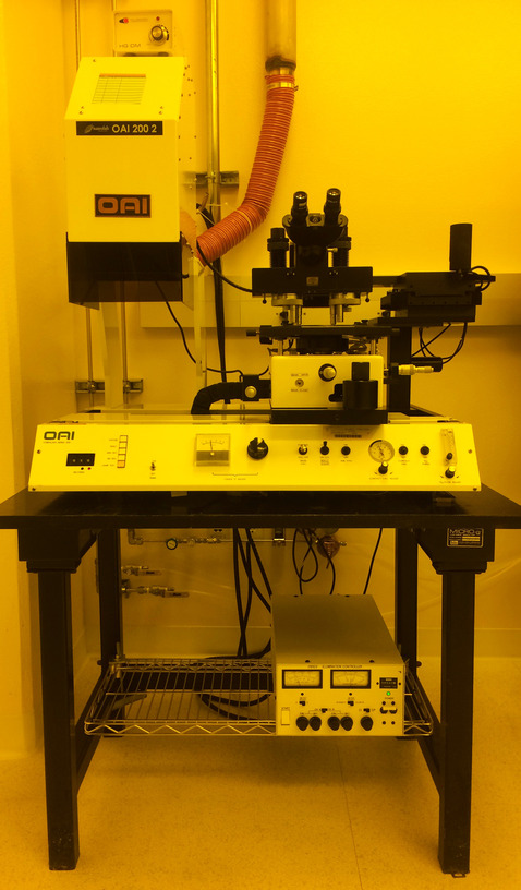
The OAI Model 200 is a tabletop mask aligner and UV exposure system designed for R&D and low-volume production.
Brooks 017-0146-01 is a prealigner manufactured by Brooks.
The Ultratech 1000 Family is a photolithography step-and-repeat 1X steppers family using the Wynne Dyson optical design.