Tokyo Electron
Mark 8
The Tokyo Electron Mark 8 is a photoresist coating and developing track system for semiconductor lithography. The Mark 8 Coater/Developer configuration includes two coat modules and two developer modules. The Mark 8 Coater/Developer features a parallel wafer flow processing software option for simultaneous coat and develop.[1]

Plate 01Replacement LCD Screens for TEL Mark 8, Mark 7, Mark Vz & ACT 8 Systems
Rite Track Equipment ServicesWatch on YouTube
Wafer size
Parallel wafer flow processing software option (simultaneous coat & develop)
Gas delivery
2 coater / 2 developer[1]
What it is
General reference — not yet source-verifiedMask aligners and associated lithography track equipment support the patterning sequence used in semiconductor fabrication. A coater applies photoresist, a developer removes selected resist after exposure, and a combined coater/developer system integrates both functions in one platform.
How it works
General reference — not yet source-verifiedThe Mark 8 family includes separate coater and developer variants as well as combined processing tools. Coating tools place a uniform resist film on the wafer surface, and developer tools complete the post exposure removal of selected resist areas that define the latent pattern.
Where it fits in the process flow
General reference — not yet source-verifiedThe Mark 8 sits in the front end lithography flow between wafer preparation and pattern transfer steps. The coater portion prepares the wafer for exposure, and the developer portion follows exposure to reveal the patterned resist image before subsequent etch or deposition processing.
Applications
General reference — not yet source-verifiedThe Mark 8 family is used for resist coating and development on semiconductor wafers. The combined coater/developer configuration is suited to integrated lithography track processing where coating and developing steps are handled on the same tool.
What do the numbers mean?
Wafer handling10
- Cassette platforms (4)[1]
- A two block system / two robots (not counting carrier station)[1]
- Coater/Developer Configuration Details
- 2 coater / 2 developer - Cassette platforms (4) - Coat Modules (2) - Hot Plates (8) - Chill Plates (9) - Wash Disk system (WDS) - A two block system / two robots - Parallel wafer flow processing software option (simultaneous coat & develop) - Semifab CD 200+4TEL Temperature & Humidity Unit - Chemical cabinet containing SMC INR-244-117B Thermocons[1]
- Software option
- Parallel wafer flow processing software option (simultaneous coat & develop)[1]
Gas & chemistry6
Configuration & options15
Vintage & configurations
Documented models & variants
| Designation | Generation | Vintage | Changes | Source |
|---|---|---|---|---|
| Tel Mark 8 Developer | — | 1993 | Developer configuration for 6-inch wafers. | Equipment inventory listing[3] |
| Tel Mark 8 Coater | — | 1992 | Coater configuration for 6-inch wafers. | Equipment inventory listing[2] |
| Tel MARK 8 | — | 1998 | 8-inch SOGT configuration. | Equipment inventory listing[5] |
| Mark 8 Developer | — | 1993 | — | Equipment inventory listing[3] |
| Mark 8 Coater | — | 1992 | — | Equipment inventory listing[2] |
| Mark 8 | — | 1998 | Listed as a coater/developer with parallel wafer flow processing software option (simultaneous coat & develop). | Equipment inventory listing[1] |
| Mark 8 Coater (6 inch) | — | 1992 | Coater-only configuration for 6-inch wafers | Equipment inventory listing[2] |
| Mark 8 Coater (8 inch) | — | 1996 | Coater-only configuration for 8-inch wafers | Equipment inventory listing[4] |
| Mark 8 SOGT | — | 1998 | SOGT variant (Spin-On-Glass Thin? or similar process) | Equipment inventory listing[5] |
| Mark 8 Coater/Developer | — | — | Combined coater and developer with parallel wafer flow processing | Equipment inventory listing[1] |
What does it need to run?
Site utility requirements, footprint, and infrastructure needed to install and operate this tool. Sourced from public records.
- Configuration2 coater / 2 developer[1]
- ConfigurationChemical cabinet that contains SMC INR-244-117B Thermocons[1]
- ConfigurationA bulk developer chemical mix station available for this system[1]
- ConfigurationsDeveloper, Coater, Coater/Developer[3]
- Chemical cabinet contentsSMC INR-244-117B Thermocons[1]
- Bulk developer chemical mix stationAvailable for this system[1]
Parts & consumables
Tracked replaceable assemblies, spares criticality, and availability status across all major subsystems. Each entry cites its source.
- Tel Mark 8 Interface ModuleIn Productionsource[10]
Where are the manuals?
Generated from public-source data on file. Enter your email to access — nothing is published; details are routed privately.
Not publicly documented
Field notes
No research found yet — worked with this tool? Share what you know.
Frequently asked questions
What wafer sizes does the Tokyo Electron Mark 8 support?
The Mark 8 is available in 6-inch (150 mm) and 8-inch (200 mm) configurations.[3][2][4][1][5]
Does the Mark 8 support simultaneous coating and developing?
Yes, the coater/developer configuration includes a parallel wafer flow processing software option that enables simultaneous coating and developing of different wafers.[1]
Is a 6-inch kit available for the 8-inch coater/developer?
Yes, the 8-inch coater/developer configuration can be equipped with a 6-inch kit to process smaller wafers.[1]
Not publicly documented
The following facts about the Mark 8 are absent from this record as of this revision. First-hand knowledge or a citation closes a gap; every submission is reviewed before publication.
The control-system platform and OS era of the Mark 8 are not on record.
Answerable by: an engineer who operated it or OEM installation records
No publicly documented failure modes or field errata for the Mark 8 are on record.
Answerable by: a field service engineer, process engineer, or maintenance technician
The process node or technology generation of the Mark 8 is not on record.
Answerable by: an OEM datasheet or a fab qualification report
No publicly hosted manuals, SOPs, or datasheets for the Mark 8 are on record.
Answerable by: university cleanroom staff or an OEM application specialist
No research found yet — worked with this tool? Share what you know.
Sources & citations
Sources (11)Every fact above is drawn from these public sources
- [1]Inventory photo
- [2]Equipment inventory listing
- [3]Equipment inventory listing
- [4]Equipment inventory listing
- [5]Equipment inventory listing
- [6]Inventory photo
- [7]Inventory photo
- [8]Inventory photo
- [9]Inventory photo
- [10]Equipment inventory listing
- [11]Equipment inventory listing
Last updated Oct 9, 2026.
Compare with similar tools
View all →Brooks 017-0146-01 is a prealigner manufactured by Brooks.
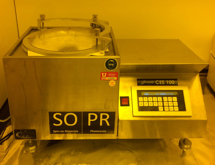
The CEE 100 is a lithography spin coater/developer tool that accepts up to 6-inch wafers and supports programmable multi-step processing.
The Ultratech 1000 Family is a photolithography step-and-repeat 1X steppers family using the Wynne Dyson optical design.