CEE
100
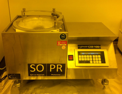
The CEE 100 is a programmable spin coater used for photoresist application in photolithography. The CEE 100 accepts wafers up to 6 inches in diameter and supports 10 programs with up to 10 steps each. The CEE 100 also exists in a spray developer configuration and a CEE 100CB spinner/hotplate variant.[1][2]
Wafer size
6"
Gas delivery
Spray Developer[2]
What it is
General reference — not yet source-verifiedThe CEE 100 is a spin coater used in photolithography. Spin coaters apply liquid photoresist or other coating fluids to a substrate by rotating the substrate so the liquid spreads into a thin film. Spin coaters are typically used in the coating stage before soft bake, alignment or exposure, development, and later pattern transfer steps.
How it works
The Cee Model 100 and 150 spinner module incorporates a stainless steel spin bowl. The spin bowl drain and exhaust connect through Teflon tubing to the main utilities bracket on the rear of the machine. The main drive spindle for the spin chuck is made of hardened corrosion-resistant alloy steel. The spindle is driven by a toothed belt and a servo motor. An integral optical encoder provides feedback for the closed-loop digital motor control system. The Cee Model 100 and 150 use a closed bowl design with an exhaust lid and a bottom exhaust port beneath the spin chuck.[4]
Where it fits in the process flow
General reference — not yet source-verifiedSpin coating sits in the lithography sequence after substrate preparation and before exposure and development. A typical flow places adhesion promotion or dehydration before coating, then uses bake steps to condition the film, followed by patterning and resist development. The coated resist can then serve as a temporary imaging layer for etch, deposition, implantation, or lift-off steps.
Applications
General reference — not yet source-verifiedSpin coaters are used to form uniform thin liquid films for photolithography and related microfabrication work. Common uses include coating positive or negative photoresists, lift-off stacks, and other solution-processed layers that must be spread evenly before later thermal or patterning steps.
- Photolithography
- Lift-off resist processing
What do the numbers mean?
Wafer handling3
Gas & chemistry1
Control & software1
Configuration & options8
Vintage & configurations
Documented models & variants
| Designation | Generation | Vintage | Changes | Source |
|---|---|---|---|---|
| CEE 100CB | — | — | Includes a hotplate; available in table top and bench mount configurations | nanofab.ece.cmu.edu[2] |
What replaced it?
What does it need to run?
Site utility requirements, footprint, and infrastructure needed to install and operate this tool. Sourced from public records.
- Tool typeSpray Developer[2]
Where are the manuals?
Generated from public-source data on file. Enter your email to access — nothing is published; details are routed privately.
Not publicly documented
Field notes
No research found yet — worked with this tool? Share what you know.
Frequently asked questions
Not publicly documented
The following facts about the 100 are absent from this record as of this revision. First-hand knowledge or a citation closes a gap; every submission is reviewed before publication.
No publicly documented production dates or lifecycle milestones (introduction, end of production, EOL) for the 100 are on record.
Answerable by: OEM historical records or a trade-press announcement
The control-system platform and OS era of the 100 are not on record.
Answerable by: an engineer who operated it or OEM installation records
No publicly documented failure modes or field errata for the 100 are on record.
Answerable by: a field service engineer, process engineer, or maintenance technician
The process node or technology generation of the 100 is not on record.
Answerable by: an OEM datasheet or a fab qualification report
No publicly documented compatible parts, consumables, or accessories for the 100 are on record.
Answerable by: an OEM parts catalog or a service engineer
No research found yet — worked with this tool? Share what you know.
Sources & citations
Sources (4)Every fact above is drawn from these public sources
- [1]nanofab.utah.edu — nanofab.utah.edunanofab.utah.edu
- [2]nanofab.ece.cmu.edu — nanofab.ece.cmu.edunanofab.ece.cmu.edu
- [3]nanofab.utah.edu — nanofab.utah.edunanofab.utah.edu
- [4]https://cense.engr.uky.edu/sites/default/files/2026-06/100-150-service-manual.pdf — cense.engr.uky.educense.engr.uky.edu
Last updated Oct 19, 2026.
Compare with similar tools
View all →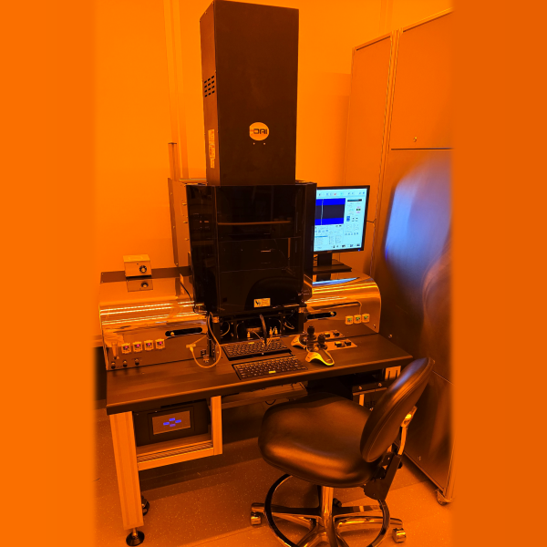
The OAI 806 Mask Aligner is a precision photolithography tool for patterning substrates up to 6 inches with soft, hard, and proximity contact modes.

Heidelberg Instruments DWL66 is a high-resolution direct write pattern generator for direct writing on various substrates and mask making.
Raith EBPG5200 is a direct write electron beam lithography system with high-kV capability and automation features stated in the product page for the EBPG line.
