KLA
Surfscan SP 2 Particle Defect
The KLA Surfscan SP 2 is a particle defect inspection system. The KLA Surfscan SP 2 provides <37 nm defect sensitivity on polished bare silicon. The KLA Surfscan SP 2 supports wafer sizes of 6, 8, and 12 inches.[1][2]

Wafer size
300mm
Vacuum
Vacuum 300mm/200mm[10]
Performance
Optimized Sensitivity & Throughput[1]
Optics
UV Laser[1]
What it is
General reference — not yet source-verifiedParticle defect inspection systems scan wafer surfaces for light-scattering events associated with particles and other surface defects. Particle defect inspection systems are used to detect contamination, map defect locations, and support yield-related monitoring in semiconductor manufacturing.
How it works
General reference — not yet source-verifiedParticle scanners of this class direct controlled illumination onto the wafer surface and detect scattered light from localized surface anomalies. Particle scanners of this class convert the detected signal into defect maps and classification data for later review and process analysis.
Where it fits in the process flow
General reference — not yet source-verifiedSurface particle inspection tools are used at monitoring points where contamination on bare or processed wafers can affect downstream yield and device performance. Surface particle inspection tools are commonly placed around substrate qualification, process qualification, and recurring line monitoring steps.
Applications
General reference — not yet source-verifiedParticle defect inspection systems are applied where fabs need to separate particulate contamination from broader surface-condition signatures and to trend defectivity over time. Particle defect inspection systems can support engineering work on substrate cleanliness, process excursions, and recurring contamination sources.
What do the numbers mean?
Vacuum & pumping4
Wafer handling7
Optics & imaging14
- <37 nm defect sensitivity on polished bare silicon[1]
- Qualification & monitoring of process tools, at the 90, 65, & 45 nm technology nodes[1]
- UV Laser[1]
- Advanced Illumination Optics Supporting the Following Mode(s):[1]
- Oblique Illumination[1]
- Included licenses
- Optical Filter, Enhanced XY Coordinates, 2 mm Edge Exclusion, Standard Classification Package, LPD-N Classification, LPD-ES Classification, Grading & Sorting, Haze, Haze Analysis & Normalization, Haze Line Classification, IDM 2011 Vintage[1]
- Included components
- UV Laser; defect map & histogram with zoom; iMicroView measurement capability; SURFimage; Real-Time Defect Classification (RTDC); Microsoft Windows XP Operating System[1]
Performance4
Control & software6
Configuration & options17
- Includes HDD[1]
- Assists in process trouble shooting & development[1]
- Includes the Following Components:[1]
- Defect map& histogram with zoom[1]
- iMicroView measurement capability[1]
- SURFimage[1]
- Real-Time Defect Classification (RTDC)[1]
- Features Following Inspection Modes:[1]
- High Sensitivity Inspection Mode[1]
- 1 Shinko Load Port / 1 Rorze Port[2]
What does it need to run?
Site utility requirements, footprint, and infrastructure needed to install and operate this tool. Sourced from public records.
- Handler TypeVacuum 300mm/200mm[10]
- Wafer handler300 mm Phoenix Dual FIMS Vacuum Wafer Handler (PP) Ballroom Configuration; Phoenix 2.0 Handler[1]
- Wafer sizeIncludes 300 mm Phoenix Dual FIMS Vacuum Wafer Handler (PP)[1]
- Handler300 mm Phoenix Dual FIMS Vacuum Wafer Handler (PP) Ballroom Configuration (Standard)[1]
Where are the manuals?
Generated from public-source data on file. Enter your email to access — nothing is published; details are routed privately.
Not publicly documented
Field notes
No research found yet — worked with this tool? Share what you know.
Frequently asked questions
What wafer sizes does the KLA Surfscan SP 2 support?
The KLA Surfscan SP 2 supports 6-, 8-, and 12-inch wafer sizes.[1][2]
What is the defect sensitivity of the Surfscan SP 2?
The system achieves a defect sensitivity of less than 37 nanometers on polished bare silicon.[1]
What illumination modes are available on the SP 2?
The Surfscan SP 2 offers oblique and normal dark-field illumination modes.[1][2]
What inspection modes does the SP 2 have?
The system includes standard throughput inspection mode and high sensitivity inspection mode.[1]
Does the Surfscan SP 2 include real-time defect classification?
Yes, the Surfscan SP 2 includes Real-Time Defect Classification (RTDC) capability.[1]
Not publicly documented
The following facts about the Surfscan SP 2 Particle Defect are absent from this record as of this revision. First-hand knowledge or a citation closes a gap; every submission is reviewed before publication.
No publicly documented production dates or lifecycle milestones (introduction, end of production, EOL) for the Surfscan SP 2 Particle Defect are on record.
Answerable by: OEM historical records or a trade-press announcement
No publicly documented variants, configuration options, or revision breakpoints of the Surfscan SP 2 Particle Defect are on record.
Answerable by: an OEM product catalog or an engineer who ordered or specified the tool
The control-system platform and OS era of the Surfscan SP 2 Particle Defect are not on record.
Answerable by: an engineer who operated it or OEM installation records
No publicly documented failure modes or field errata for the Surfscan SP 2 Particle Defect are on record.
Answerable by: a field service engineer, process engineer, or maintenance technician
The process node or technology generation of the Surfscan SP 2 Particle Defect is not on record.
Answerable by: an OEM datasheet or a fab qualification report
No research found yet — worked with this tool? Share what you know.
Sources & citations
Sources (11)Every fact above is drawn from these public sources
- [1]Inventory photo
- [2]Inventory photo
- [3]Inventory photo
- [4]Inventory photo
- [5]Inventory photo
- [6]Inventory photo
- [7]Inventory photo
- [8]Inventory photo
- [9]Inventory photo
- [10]waferpedia.comwaferpedia.com
- [11]Equipment inventory listing
Last updated Oct 20, 2026.
Compare with similar tools
View all →The Rudolph E25 System is an automated wafer edge top and edge normal inspection system for 300 mm wafers.
The Sonoscan Gen-6 is a C-mode Scanning Acoustic Microscope with scanning capability for JEDEC trays or a 300mm wafer.
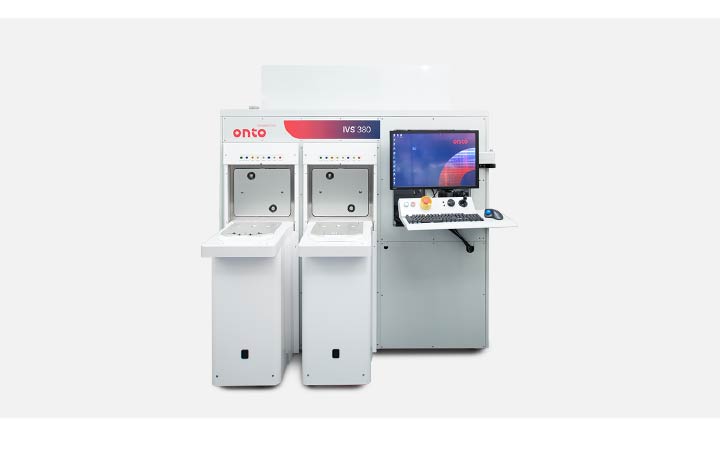
The IVS 380 System performs overlay, CD, and height metrology for 300mm wafers.
The KLA .204 PSL Wafer is an 8-inch NIST-traceable reference wafer compatible with Surfscan 6xy0 and Sp1 particle counters.