Perkin Elmer
Micralign
The Micralign is a family of projection aligners introduced in 1973 by Perkin-Elmer. The Micralign was the first projection aligner, and it dramatically improved semiconductor fabrication yields. The Micralign uses a scanning mirror system to project the mask image onto the wafer.[1]
Plate 01AIM Micralign Perkin Elmer display
Capetronics IncWatch on YouTubePlate 02MICRALIGN PERKIN ELMER LED DISPLAY
Luong TranWatch on YouTube
Wafer size
2-inch, 2.5-inch, or 3-inch wafers; optionally 4×4-inch, 3.5×3.5-inch, or 3×3-inch masks
Produced
1971–1990
Optics
4×4-inch, 3.5×3.5-inch, or 3×3-inch masks[1]
What it is
The Perkin Elmer Micralign is a lithography aligner used in semiconductor fabrication. The Micralign was a family of aligners introduced in 1973 by Perkin-Elmer. The Micralign was the first projection aligner. The Micralign used a 1:1 scanning projection system to address limitations of contact mask aligners.[1][2]
How it works
The Perkin Elmer Micralign exposes photoresist by projection rather than by direct mask contact. The Micralign used a 1:1 scanning projection system. The Micralign family originated from Perkin-Elmer work on a higher-resolution aligner under a 1967 US Air Force contract. The earlier Microprojector effort used a 16-element lens system and demonstrated 2.5 μm features.[1][2]
Where it fits in the process flow
Photolithography occurs as a repeated patterning sequence within wafer fabrication. A wafer is coated with photoresist before exposure, and the developed resist pattern is then used in subsequent chemical processing to impart the intended electrical structure. Each layer uses a different mask, and each new pattern must be aligned to patterns already deposited on the wafer.[1]
Applications
The Perkin Elmer Micralign was developed for integrated circuit manufacturing. The Micralign addressed yield problems associated with earlier contact aligners, and the improvement supported more practical production of complex integrated circuits such as microprocessors and dynamic RAM devices.[1]
- Semiconductor fabrication
- Photolithography
Why won't it start?
Documented failure modes, common issues, and field considerations.
- Contact aligners suffered from dust contamination on masks.
- Contact masks could stick to uncured photoresist and damage wafers.
- Thermal expansion during longer exposures required a change from soda-lime glass to borosilicate glass for masks.
- The earlier Microprojector used filters that reduced visible light, making alignment difficult without an added image intensifier.
What do the numbers mean?
Wafer handling1
Optics & imaging1
Configuration & options7
Vintage & configurations
- 1971Production start[1]
A production team for the practical design was formed in May 1971.
- 1973Production start[1]
Micralign family introduced by Perkin-Elmer.
- 1973Introduction[1]
Micralign introduced in 1973.
- 1974Production start[1]
First sale of the Micralign 100 was to Texas Instruments.
- 1990Divestiture[1]
Perkin-Elmer sold the division in 1990.
- 1990Production end[1]
Perkin-Elmer sold the division to Silicon Valley Group.
Documented models & variants
| Designation | Generation | Vintage | Changes | Source |
|---|---|---|---|---|
| Micralign 100 | — | 1974 | First sale of the line’s Micralign 100 model was in 1974. | en.wikipedia.org[1] |
| Model 110 | — | — | Added an automated wafer loader. | en.wikipedia.org[1] |
| Model 111 | — | — | Single-wafer model that replaced the 100; could be adapted for use with 2-, 2.5- or 3-inch wafers and optionally 4×4-, 3.5×3.5- or 3×3-inch masks. | en.wikipedia.org[1] |
| Model 120 | — | — | A 111 with automatic wafer loading. | en.wikipedia.org[1] |
| Model 130 | — | — | Worked with 100 mm wafers and 5×5-inch masks. | en.wikipedia.org[1] |
| Model 140 | — | — | Added wafer loading to the 130. | en.wikipedia.org[1] |
Where are the manuals?
Generated from public-source data on file. Enter your email to access — nothing is published; details are routed privately.
Not publicly documented
Field notes
No research found yet — worked with this tool? Share what you know.
Frequently asked questions
What type of lithography tool is the Perkin Elmer Micralign?
The Perkin Elmer Micralign is a projection aligner used in semiconductor fabrication. The Micralign was the first projection aligner, and it used a 1:1 scanning projection system.[1][2]
When was the Micralign introduced?
The Micralign family was introduced in 1973 by Perkin-Elmer.[1]
What problem did the Micralign address compared with contact mask aligners?
The Micralign addressed problems associated with contact mask aligners, including defects caused by physical contact between the mask and wafer and limitations in yield. The Micralign used projection exposure to address some of those issues.[1][2]
How does the Micralign fit into the wafer fabrication flow?
The Micralign is used during photolithography. In that flow, wafers are coated with photoresist, exposed through a mask, developed, and then subjected to subsequent chemical processing. Each masking step uses a different mask and must be aligned to previous layers on the wafer.[1]
Not publicly documented
The following facts about the Micralign are absent from this record as of this revision. First-hand knowledge or a citation closes a gap; every submission is reviewed before publication.
The control-system platform and OS era of the Micralign are not on record.
Answerable by: an engineer who operated it or OEM installation records
The process node or technology generation of the Micralign is not on record.
Answerable by: an OEM datasheet or a fab qualification report
No publicly documented compatible parts, consumables, or accessories for the Micralign are on record.
Answerable by: an OEM parts catalog or a service engineer
No publicly hosted manuals, SOPs, or datasheets for the Micralign are on record.
Answerable by: university cleanroom staff or an OEM application specialist
Sources & citations
Sources (2)Every fact above is drawn from these public sources
- [1]en.wikipedia.org — en.wikipedia.orgen.wikipedia.org
- [2]Stepper Training Manual - REQUIRED READING — cnfusers.cornell.educnfusers.cornell.edu
Last updated Oct 20, 2026.
Compare with similar tools
View all →Brooks 017-0146-01 is a prealigner manufactured by Brooks.
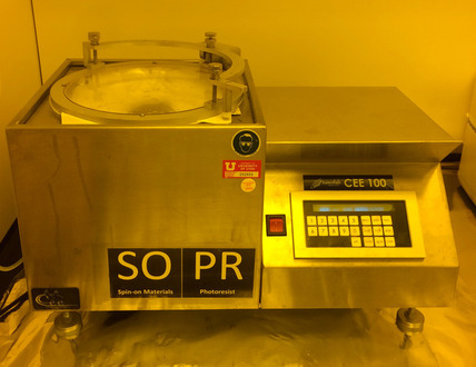
The CEE 100 is a lithography spin coater/developer tool that accepts up to 6-inch wafers and supports programmable multi-step processing.
The Ultratech 1000 Family is a photolithography step-and-repeat 1X steppers family using the Wynne Dyson optical design.