SUSS MicroTec
MA 6 Mask

Plate 01Exposure using contact aligner (Suss MA6)
Micro System Integration Center(uSIC), Tohoku UnivWatch on YouTubePlate 02Karl Suss MA6 Mask Aligner - Standard Operating Procedures
InrfucirvineWatch on YouTube
Power
1000 Watt Power Supply[2]
Performance
with Infrared Alignment[7]
Optics
IR Back Side Illumination[2]
What it is
General reference — not yet source-verifiedA mask aligner is a lithography tool that aligns a patterned mask to a substrate and exposes photoresist so the pattern can be transferred. Mask aligners are used in microfabrication flows where contact or proximity exposure is suitable and where direct optical alignment of mask and wafer is part of the process.
How it works
General reference — not yet source-verifiedMask aligners position a substrate beneath a mask, bring the two into a defined alignment condition, and expose the resist-coated surface with ultraviolet light. Alignment optics let the operator register mask features to wafer features before exposure, and the exposure step defines the resist image used by later development and pattern transfer steps.
Where it fits in the process flow
General reference — not yet source-verifiedMask aligners sit at the photolithography stage of a microfabrication process. A mask aligner is typically used after substrate preparation and photoresist coating, and before resist development, etching, deposition lift-off, or other pattern transfer operations.
Mask aligners are commonly used when a process flow needs patterned resist on wafers or other flat substrates without the projection-optics architecture of a stepper or scanner. Mask aligners are often selected for process modules that depend on overlay to existing features, including flows that can benefit from backside or infrared alignment capability.
Applications
General reference — not yet source-verifiedMask aligners are used for creating patterned photoresist layers in semiconductor, microsystem, and related cleanroom fabrication. Typical uses include etch masks, implant masks, plating molds, liftoff patterns, dielectric patterning, and alignment-sensitive layers on substrates that carry previously formed structures.
What do the numbers mean?
Power & electrical11
- 1000 Watt Power Supply[2]
- 50/60 Hz[7]
- 200–240V, 50/60Hz[8]
- Product Details
- up to 6" - 50/60 Hz - 230 V - HDD - Software - with Infrared Alignment - No BSA 2001 Vintage[7]
- Product Details
- 6" - 200–240V, 50/60Hz - 7-inch air chuck - UV lamp power supply: CIC1200/157308LS Topside alignment objectives (2): - MplanFL N 5x/0.15 - MplanFL N 10x/0.30 - LMPlanFL N 20x/0.40 2008 Vintage[8]
Wafer handling8
Optics & imaging6
Performance2
- with Infrared Alignment[7]
Control & software1
- Software[7]
Configuration & options9
What replaced it?
Alternatives
Tools documented as functional equivalents — same process step and wafer size, from a different manufacturer. Each equivalence cites its source.
- OAI 200— Same function class: Lithography, nullCompare in depthsource[9]
- Canon FPA 3000 i 5 + Fine Pattern— Same function class: Lithography, nullCompare in depthsource[10]
- OAI 806 Mask— Same function class: Lithography, nullCompare in depthsource[9]
- Canon FPA 3000 i 4— Same function class: Lithography, nullCompare in depthsource[9]
What does it need to run?
Site utility requirements, footprint, and infrastructure needed to install and operate this tool. Sourced from public records.
- Configuration1000 Watt Power Supply[2]
- Configuration50/60 Hz[7]
- Voltage230 V[7]
- Configuration200–240V, 50/60Hz[8]
- UV lamp power supplyCIC1200/157308LS[8]
- Power Supply1000 Watt[2]
- Voltage / Frequency200-240V, 50/60Hz[8]
- Product Detailsup to 6" - 50/60 Hz - 230 V - HDD - Software - with Infrared Alignment - No BSA 2001 Vintage[7]
- Product Details6" - 200–240V, 50/60Hz - 7-inch air chuck - UV lamp power supply: CIC1200/157308LS Topside alignment objectives (2): - MplanFL N 5x/0.15 - MplanFL N 10x/0.30 - LMPlanFL N 20x/0.40 2008 Vintage[8]
- Power supply1000 Watt Power Supply[2]
- Voltage200–240V[8]
Where are the manuals?
Publicly hosted documents referencing this tool, linked at their original location. Hosted by the linked institutions — availability may change.
- ManualManualuic.edu
Generated from public-source data on file. Enter your email to access — nothing is published; details are routed privately.
Not publicly documented
Field notes
No research found yet — worked with this tool? Share what you know.
Frequently asked questions
Not publicly documented
The following facts about the MA 6 Mask are absent from this record as of this revision. First-hand knowledge or a citation closes a gap; every submission is reviewed before publication.
No publicly documented production dates or lifecycle milestones (introduction, end of production, EOL) for the MA 6 Mask are on record.
Answerable by: OEM historical records or a trade-press announcement
No publicly documented variants, configuration options, or revision breakpoints of the MA 6 Mask are on record.
Answerable by: an OEM product catalog or an engineer who ordered or specified the tool
The control-system platform and OS era of the MA 6 Mask are not on record.
Answerable by: an engineer who operated it or OEM installation records
No publicly documented failure modes or field errata for the MA 6 Mask are on record.
Answerable by: a field service engineer, process engineer, or maintenance technician
The process node or technology generation of the MA 6 Mask is not on record.
Answerable by: an OEM datasheet or a fab qualification report
No research found yet — worked with this tool? Share what you know.
Sources & citations
Sources (16)Every fact above is drawn from these public sources
- [1]Inventory photo
- [2]Inventory photo
- [3]Inventory photo
- [4]Inventory photo
- [5]Inventory photo
- [6]Inventory photo
- [7]inventory listing
- [8]inventory listing
- [9]Exposure | Stanford Nanofabrication Facility — snfguide.stanford.edusnfguide.stanford.edu
- [10]Equipment inventory listing
- [11]Equipment inventory listing
- [12]Karl Suss MA6 Mask Aligner | Nanotechnology Core Facility | University of Illinois Chicago — ncf.uic.eduncf.uic.edu
- [13]Suss MA6 Mask Aligner (system 2) — tmi.utexas.edutmi.utexas.edu
- [14]Tool Details - Harvard CNS — cns1.rc.fas.harvard.educns1.rc.fas.harvard.edu
- [15]Frontside/Backside Mask Aligner | Shared Materials Instrumentation Facility — smif.pratt.duke.edusmif.pratt.duke.edu
- [16]ece.utoronto.ca — ece.utoronto.caece.utoronto.ca
Last updated Oct 20, 2026.
Compare with similar tools
View all →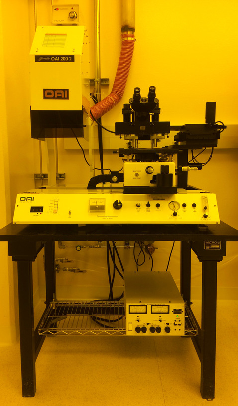
The OAI Model 200 is a tabletop mask aligner and UV exposure system designed for R&D and low-volume production.
The OAI 806 Mask Aligner is a manual wafer load mask aligner used for photolithography, supporting wafer sizes up to 6 inches with submicron alignment accuracy.

The Canon FPA 3000 i 4 is a lithography stepper or fine pattern aligner for semiconductor wafer pattern transfer.
