SUSS MicroTec
MA6/MA4
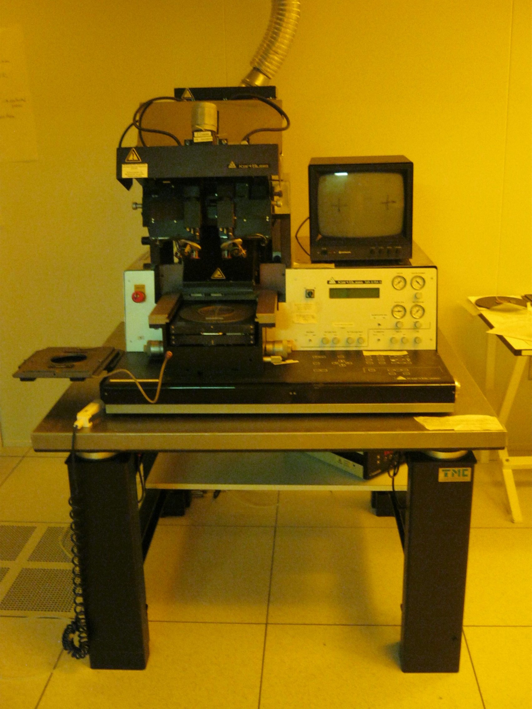
The SUSS MicroTec MA6/MA4 is a UV mask aligner line. The SUSS MicroTec MA6/MA4 uses UV light to transfer patterns from photomasks onto photoresist-coated substrates. The SUSS MicroTec MA6/MA4 accommodates wafers up to 4″ on MA4 and up to 6″ on MA6, and also 1 cm² pieces.[1]
Wafer size
wafers up to 4″ (MA4) or 6″ (MA6); also 1 cm² pieces
Optics
< 1 µm[1]
What it is
The SUSS MicroTec MA6/MA4 is a mask aligner used in photolithography. The SUSS MicroTec MA6/MA4 uses UV light to transfer patterns from photomasks onto substrates coated with photoresist. The MA4 accommodates wafers up to 4 inches, while the MA6 accommodates wafers up to 6 inches. The MA6 and MA4 also accommodate 1 cm2 pieces.[1][3][2]
How it works
The SUSS MicroTec MA6/MA4 uses exposure modes that include hard contact, soft contact, proximity, and flood. The SUSS MicroTec MA6/MA4 operates over a spectral range of 365 nm to 405 nm. The SUSS MicroTec MA6/MA4 has exposure resolution below 1 µm. The SUSS MicroTec MA6/MA4 has topside alignment accuracy of 500 nm. The SUSS MicroTec MA6/MA4 includes a CCD camera and monitor for image capture. The SUSS MicroTec MA6/MA4 has uniformity of plus or minus 5 percent over the exposure area.[1][3]
Where it fits in the process flow
General reference — not yet source-verifiedPhotolithography tools of this class sit at the pattern-definition stage of microfabrication. A mask aligner is typically used after substrate cleaning, dehydration, and photoresist coating with a soft bake, and before development and the follow-on pattern transfer or lift-off step. The patterned resist produced by the exposure step serves as a temporary stencil for later deposition, etch, plating, or surface modification operations.
Applications
General reference — not yet source-verifiedMask aligners are used to create patterned resist layers for microscale fabrication on wafers and small substrates. Typical uses include defining structures for etching, deposition patterning, lift-off, surface treatment, and mold or stamp fabrication in research and pilot-line work.
- Transferring patterns from photomasks onto photoresist-coated substrates
What do the numbers mean?
Wafer handling2
Optics & imaging7
Vintage & configurations
Where are the manuals?
Generated from public-source data on file. Enter your email to access — nothing is published; details are routed privately.
Not publicly documented
Field notes
No research found yet — worked with this tool? Share what you know.
Frequently asked questions
Not publicly documented
The following facts about the MA6/MA4 are absent from this record as of this revision. First-hand knowledge or a citation closes a gap; every submission is reviewed before publication.
No publicly documented production dates or lifecycle milestones (introduction, end of production, EOL) for the MA6/MA4 are on record.
Answerable by: OEM historical records or a trade-press announcement
The control-system platform and OS era of the MA6/MA4 are not on record.
Answerable by: an engineer who operated it or OEM installation records
No publicly documented failure modes or field errata for the MA6/MA4 are on record.
Answerable by: a field service engineer, process engineer, or maintenance technician
The process node or technology generation of the MA6/MA4 is not on record.
Answerable by: an OEM datasheet or a fab qualification report
No publicly documented compatible parts, consumables, or accessories for the MA6/MA4 are on record.
Answerable by: an OEM parts catalog or a service engineer
No research found yet — worked with this tool? Share what you know.
Sources & citations
Sources (3)Every fact above is drawn from these public sources
- [1]ece.utoronto.ca — ece.utoronto.caece.utoronto.ca
- [2]waferpedia.com — waferpedia.comwaferpedia.com
- [3]MA6/MA4 — SUSS MicroTec | Specs, Sourcing & Service | Waferpedia — waferpedia.comwaferpedia.com
Last updated Oct 17, 2026.
Compare with similar tools
View all →Brooks 017-0146-01 is a prealigner manufactured by Brooks.
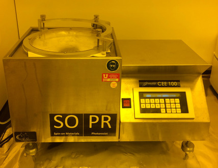
The CEE 100 is a lithography spin coater/developer tool that accepts up to 6-inch wafers and supports programmable multi-step processing.
The Ultratech 1000 Family is a photolithography step-and-repeat 1X steppers family using the Wynne Dyson optical design.