Heidelberg Instruments
DWL66
The Heidelberg Instruments DWL66 is an economical, high-resolution direct-write pattern generator. The Heidelberg Instruments DWL66 is suitable for rapid prototyping of 2D and 3D microstructures on substrates up to 6 inches square. The Heidelberg Instruments DWL66 lists laser sources at 244 nm, 363 nm, 413 nm, and 442 nm.[1]

Plate 01Replacing Photomasks with Direct Write Lithography | DWL 66⁺ User Interview at Koç University
Heidelberg InstrumentsWatch on YouTubePlate 02How the Sydney Nano Foundry Uses the DWL 66⁺ Laser Lithography System
Heidelberg InstrumentsWatch on YouTubePlate 03Heidelberg DWL66+ Tool Training Part 3, Running the Exposure
Quattrone Nanofabrication FacilityWatch on YouTubePlate 04Heidelberg DWL66+ Tool Training Part 1, Introduction
Quattrone Nanofabrication FacilityWatch on YouTubePlate 05Laser Writer DWL66+ LIT 027 Basic Exposure Training
NanofabricationWatch on YouTubePlate 06DWL 66 Exposure
Grey1024Watch on YouTube
Wafer size
6"
Power
230 VAC ± 5%, 50/60 Hz, 16 A[1]
Gas delivery
photoresist[1]
Optics
40 nm, 100 nm, 200 nm, 400 nm[1]
What it is
General reference — not yet source-verifiedDirect-write lithography systems pattern resist without a photomask by steering or scanning a writing beam across a coated substrate. Direct-write lithography systems are commonly used where design flexibility, rapid iteration, or limited mask volume is more important than the throughput of projection exposure. Direct-write lithography systems commonly serve research, prototyping, and specialized microfabrication work.
How it works
General reference — not yet source-verifiedMaskless laser writers generally operate by coating a substrate with photoresist, loading the substrate onto a precision stage, aligning the pattern to substrate marks when needed, and scanning a focused beam to define the layout. Maskless laser writers generally rely on motion control, focusing, and exposure control to transfer digital layout data into resist. Maskless laser writers can also support overlay work and topographic patterning modes when equipped with alignment or grayscale functions.
Where it fits in the process flow
General reference — not yet source-verifiedDirect-write lithography tools are used after substrate preparation and photoresist coating, and before resist development and any subsequent etch, deposition, plating, or lift-off sequence. Direct-write lithography tools fill the pattern-definition step in a microfabrication flow. Direct-write lithography tools are often selected when a process requires short design-turn cycles or frequent layout changes.
Applications
General reference — not yet source-verifiedDirect-write laser lithography is commonly used for research patterning, mask fabrication, and custom microdevice development. Direct-write laser lithography is suitable for work that benefits from digital pattern generation on resist-coated substrates. Direct-write laser lithography is also used for structures that need iterative design changes or specialized alignment strategies.
- Reticles
- ASICs
- MEMS
- TFTs
- Sensors
- MCMs
- Integrated Optics
- MOEMS
- refractive optics
- diffractive optics
- Micro Fluidics
What do the numbers mean?
Power & electrical1
Wafer handling3
Gas & chemistry1
Optics & imaging2
Dimensions & facilities2
Configuration & options3
Vintage & configurations
Documented models & variants
| Designation | Generation | Vintage | Changes | Source |
|---|---|---|---|---|
| DWL 66 fs | — | — | Described as a high accuracy maskless lithography system; accommodates substrate size up to 200 mm by 200 mm and can expose features down to 0.6 microns. | web.archive.org[2] |
What does it need to run?
Site utility requirements, footprint, and infrastructure needed to install and operate this tool. Sourced from public records.
Where are the manuals?
Generated from public-source data on file. Enter your email to access — nothing is published; details are routed privately.
Not publicly documented
Field notes
No research found yet — worked with this tool? Share what you know.
Frequently asked questions
Does the DWL66 offer alignment or grayscale options?
The DWL66 can optionally be equipped with an alignment system that includes front to backside alignment and a grayscale exposure mode. The DWL 66 fs also lists possible options including metrology, layer to layer alignment, front to back side alignment, and grey scale exposure.[1][2]
Not publicly documented
The following facts about the DWL66 are absent from this record as of this revision. First-hand knowledge or a citation closes a gap; every submission is reviewed before publication.
No publicly documented production dates or lifecycle milestones (introduction, end of production, EOL) for the DWL66 are on record.
Answerable by: OEM historical records or a trade-press announcement
The control-system platform and OS era of the DWL66 are not on record.
Answerable by: an engineer who operated it or OEM installation records
No publicly documented failure modes or field errata for the DWL66 are on record.
Answerable by: a field service engineer, process engineer, or maintenance technician
The process node or technology generation of the DWL66 is not on record.
Answerable by: an OEM datasheet or a fab qualification report
No publicly documented compatible parts, consumables, or accessories for the DWL66 are on record.
Answerable by: an OEM parts catalog or a service engineer
No research found yet — worked with this tool? Share what you know.
Sources & citations
Sources (2)Every fact above is drawn from these public sources
- [1]web.archive.org — web.archive.orgweb.archive.org
- [2]web.archive.org — web.archive.orgweb.archive.org
Last updated Oct 16, 2026.
Compare with similar tools
View all →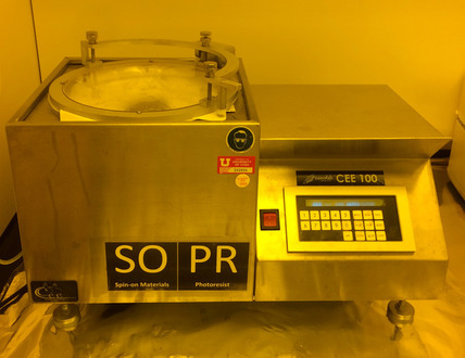
The CEE 100 is a lithography spin coater/developer tool that accepts up to 6-inch wafers and supports programmable multi-step processing.
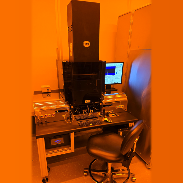
The OAI 806 Mask Aligner is a precision photolithography tool for patterning substrates up to 6 inches with soft, hard, and proximity contact modes.
Raith EBPG5200 is a direct write electron beam lithography system with high-kV capability and automation features stated in the product page for the EBPG line.
