SPTS
Rapier
The SPTS Rapier is an optimized Deep Reactive Ion Etching (DRIE) system for silicon and silicon-on-insulator wafers. The SPTS Rapier features a dual high-density Inductively Coupled Plasma source and a patented dual plasma source module with two RF-independent sources. The SPTS Rapier supports wafer biasing in radio or low frequency modes with pulsing capability.[1]
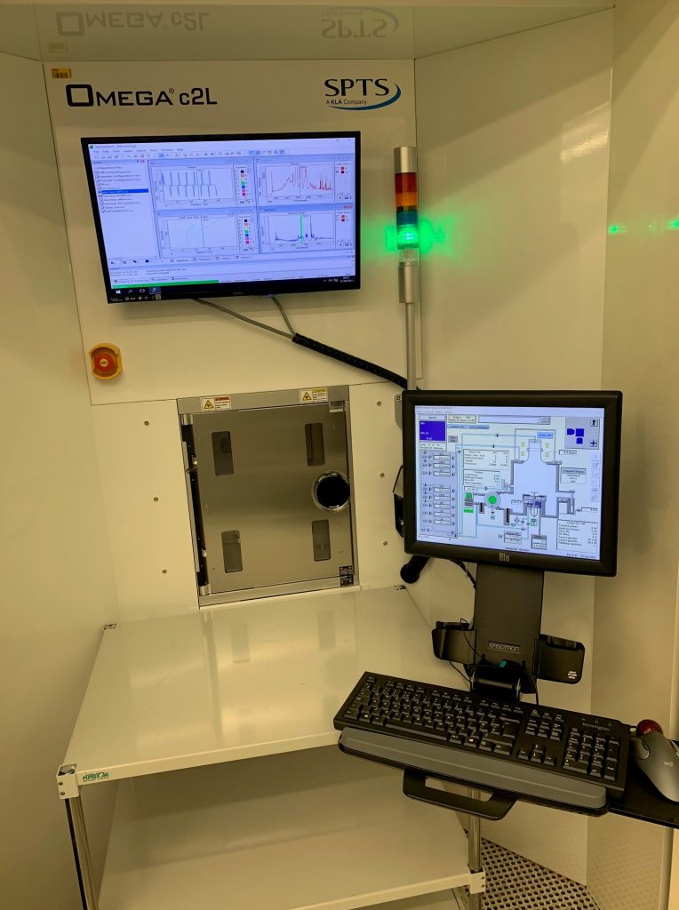
Plate 01yippeee rapier :3 #hema #historicalfencing #sca #sword #rapier
ItsParkerWatch on YouTubePlate 02🤺 rapier fencing lesson : thrust parry cut ⚔️ #defense #sword #milwaukee @cfsmke
Discovered Fencers MKEWatch on YouTubePlate 03HEMA RAPIER - Can Rapiers cut?? Sources say sure
Kyle ThrushWatch on YouTubePlate 04⚔️ Counter-Parry & Riposte by Disengagement & Yielding Glide #rapier #historicalfencing #swordplay
Boston Academie d'ArmesWatch on YouTubePlate 05SPT in Rapier & Dagger 2021 - John Leggett
John LeggettWatch on YouTubePlate 06Italian Rapier vs Sports Epee | HEMA vs Sport fencing | Weapon Confrontations - part 1
Akademia SzermierzyWatch on YouTubePlate 07HEMA Rapier- Squinter from Longpoint
Kyle ThrushWatch on YouTubePlate 08⚔️ Yielding Parry & Circular Cut #stramazzone #historicalfencing #fencingtactics #pennsic #rapier
Justin Aucoin - Historical SwordplayWatch on YouTubePlate 09Sunbeam Rapier Series V (Series 5) - the rare 1960s British sporting saloon!
idriveaclassicWatch on YouTubePlate 10JT Atwood Rapier and Dagger SPT 2024
JT AtwoodWatch on YouTube
Wafer size
Silicon and Silicon on Insulator (SOI) wafers
Power
Up to 3 kW each (two sources)[1]
Vacuum
25 wafers (single vacuum cassette loader)[1]
Gas delivery
High speed digital mass flow controllers[1]
What it is
The SPTS Rapier is a deep reactive ion etching system for silicon and silicon on insulator wafers. The SPTS Rapier is a dry etch tool used for deep silicon pattern transfer in microfabrication.[1][3][4][5]
How it works
The SPTS Rapier uses a dual high density inductively coupled plasma source, electrostatic clamping, and radio frequency or low frequency wafer biasing. The tool includes dual independent gas inlets and separate center and edge gas showers for control of plasma distribution and uniformity.[1][4][5]
The SPTS Rapier supports Bosch switched processing and non-switched etching for tapered profiles, wafer thinning, and via reveal. The tool also uses endpoint detection and process control functions for controlled etch progression.[5]
Where it fits in the process flow
Applications
The SPTS Rapier is used for deep silicon structures in microelectromechanical systems, advanced packaging, power semiconductor work, and radio frequency integrated circuit fabrication. The tool is also used for micro pillars, nano pillars, micro trenches, nano trenches, via etch, through wafer via etch, and wafer thinning.[5][4]
The SPTS Rapier is used on silicon and silicon on insulator wafers, and it supports process families for deep reactive ion etching, high aspect ratio features, optical etch variants, isotropic silicon release, oxide reactive ion etching, anti reflective coating opening, wafer thinning, and plasma dicing related work.[1]
- Deep reactive ion etching of silicon and silicon-on-insulator wafers
- Trench etching
- Hole etching
- Nano-pulsed etching
- Optical etching
- Silicon release
- Oxide RIE
- BARC opening
- Wafer thinning
- Dicing
Why won't it start?
Documented failure modes, common issues, and field considerations.
- The source notes that etch rates are design dependent and reduce with time and increasing aspect ratio (ARDE).
- For the HAR hole process, the source states the last 300 nm of mask is not viable because of faceting.
- For the Dicing process, the source states it is not for structures smaller than 10 µm due to too large CD loss.
What do the numbers mean?
Power & electrical9
Vacuum & pumping3
Wafer handling17
Gas & chemistry6
- Available process gases
- 2x SF6 720 sccm; 2x C4F8 500 sccm; O2 300 sccm and 1000 sccm; Ar 500 sccm; N2 100 sccm[1]
- Process gases
- SF6 (2x720sccm), C4F8 (2x500sccm), O2 (300sccm & 1000sccm), Ar (500sccm), N2 (100sccm)[1]
- Process Gases
- 2x SF6 (720sccm), 2x C4F8 (500sccm), O2 (300sccm & 1000sccm), Ar (500sccm), N2 (100sccm)[1]
Optics & imaging10
- Endpoint systems
- Amplified optical emission spectroscopy endpoint system; white light interferometry endpoint system[1]
- Standard process: DRIE-Nano Trench
- 350 nm: 150 nm/loop; scallops <50 nm; depth limited to tens of µm[1]
- Standard process: Opto
- From 130 nm/min to 370 nm/min; continuous etch process; for shallow and accurate etch; less than 2 µm deep[1]
- Standard process: Oxide_RIE
- SiO2: 235 nm/min; Si3N4: 110 nm/min; PR etch rate 170 nm/min; thin layers only (<1 µm); O2 cleaning compulsory[1]
- Standard process: BARC DUV42P
- 78 nm/min; Si: 50 nm/min; anti-reflective coating opening after DUV litho[1]
- Endpoint detection
- Amplified optical emission spectroscopy endpoint system and white light interferometry endpoint system[1]
- Endpoint systems
- Amplified optical emission spectroscopy endpoint system and white light interferometry endpoint system[1]
Control & software4
Configuration & options12
What replaced it?
Related models
- siblingAlcatel AMS 200 SE— Listed in the same etching equipment section.source[2]
What does it need to run?
Site utility requirements, footprint, and infrastructure needed to install and operate this tool. Sourced from public records.
- Loader capacitySingle vacuum cassette loader, 25 wafers capacity[1]
- Mass flow controllersHigh speed digital mass flow controllers[1]
- RF sourcesTwo RF independent sources, up to 3 kW each[1]
- Gas showersTwo independent gas showers (center and edge zones)[1]
- RF wafer biasingUp to 2 kW with pulsing possibility and duty cycle control[1]
- Low frequency wafer biasingUp to 1.2 kW with pulsing possibility and duty cycle control[1]
- Available process gases2x SF6 720 sccm; 2x C4F8 500 sccm; O2 300 sccm and 1000 sccm; Ar 500 sccm; N2 100 sccm[1]
- RF source powerUp to 3 kW each (two sources)[1]
- Process gasesSF6 (2x720sccm), C4F8 (2x500sccm), O2 (300sccm & 1000sccm), Ar (500sccm), N2 (100sccm)[1]
- Module sourcesTwo RF independent sources up to 3 kW[1]
- Gas showersTwo independent gas showers for center and edge zones[1]
- Clamp voltageVariable clamp voltage[1]
- Wafer Capacity25 wafers (single vacuum cassette loader)[1]
- RF Power per SourceUp to 3kW[1]
- Wafer BiasingRF up to 2kW or low frequency up to 1.2kW, with pulsing[1]
- Process Gases2x SF6 (720sccm), 2x C4F8 (500sccm), O2 (300sccm & 1000sccm), Ar (500sccm), N2 (100sccm)[1]
- Cassette loaderSingle vacuum cassette loader[1]
- Module plasma sourcesTwo RF independent sources, up to 3 kW each[1]
Where are the manuals?
Generated from public-source data on file. Enter your email to access — nothing is published; details are routed privately.
Not publicly documented
Field notes
No research found yet — worked with this tool? Share what you know.
Frequently asked questions
What is the maximum RF power for each plasma source?
Each of the two RF sources can deliver up to 3 kW.[1]
Can the tool etch sub-micron features?
Yes, it supports nano-pulsed processes for features as small as 330 nm wide.[1]
What is the typical etch rate for deep silicon trenches?
For trenches deeper than 200 micrometers, the etch rate is approximately 800 nm per loop.[1]
Not publicly documented
The following facts about the Rapier are absent from this record as of this revision. First-hand knowledge or a citation closes a gap; every submission is reviewed before publication.
No publicly documented production dates or lifecycle milestones (introduction, end of production, EOL) for the Rapier are on record.
Answerable by: OEM historical records or a trade-press announcement
No publicly documented variants, configuration options, or revision breakpoints of the Rapier are on record.
Answerable by: an OEM product catalog or an engineer who ordered or specified the tool
The control-system platform and OS era of the Rapier are not on record.
Answerable by: an engineer who operated it or OEM installation records
The process node or technology generation of the Rapier is not on record.
Answerable by: an OEM datasheet or a fab qualification report
No publicly documented compatible parts, consumables, or accessories for the Rapier are on record.
Answerable by: an OEM parts catalog or a service engineer
Sources & citations
Sources (5)Every fact above is drawn from these public sources
- [1]epfl.ch — epfl.chepfl.ch
- [2]epfl.chepfl.ch
- [3]Dry Etching — tudelft.nltudelft.nl
- [4]Tool Details - Harvard CNS — cns1.rc.fas.harvard.educns1.rc.fas.harvard.edu
- [5]SPTS Si DRIE processes — spts.com (Apr 25, 2018)web.archive.org
Last updated Oct 8, 2026.
Compare with similar tools
View all →The Applied Materials 0010-47763 is an electrostatic chuck (ESC) assembly used in semiconductor etching processes.
The Applied Materials 0010-16392 is an electrostatic chuck assembly designed for 300 mm wafer processing, featuring a dual electrode configuration.
Oxford Instruments 100 ICP Fluorine is an inductively coupled plasma etcher for fluorine-based etching, supporting cryo DRIE and multiple etch gases including SF6 and C4F8.
