Karl Suss
MJB-3
The MJB-3 is a Karl Suss mask aligner. The MJB-3 is a contact/proximity aligner. The MJB-3 can be set to utilize either 365 nm or 405 nm light.[1][2]
Plate 01Suss MJB3 350W Mask Aligner (ID 3885)
ClassOneEngineeringWatch on YouTubePlate 02Karl Suss MJB-3 HP/ST Inv# 59511
Bid ServicellcWatch on YouTubePlate 03Karl Suss MJB3 Mask Aligner #60007
Bid ServicellcWatch on YouTubePlate 04Suss MJB3 350W BSA IR Mask Aligner (ID# 3845)
ClassOneEngineeringWatch on YouTubePlate 05MNTL Karl Suss MJB3 Aligner training
cleanroom MNTLWatch on YouTubePlate 06Karl Suss MJB3 UV Intensity Measurement and Verification Supplement
Bid ServicellcWatch on YouTubePlate 07Karl Suss MJB3 Mask Aligner #59510
Bid ServicellcWatch on YouTubePlate 08Karl Suss MJB3 Aligner #60414
Bid ServicellcWatch on YouTube
Wafer size
3"
Optics
365 nm or 405 nm[1]
What it is
How it works
Where it fits in the process flow
The MJB-3 is used after photoresist is applied to the substrate. The MJB-3 supports standard photoresist processing in a teaching cleanroom workflow.[2][3]
Applications
The MJB-3 is used with a variety of positive and negative photoresists. The MJB-3 supports lithographic pattern transfer for small substrates and sample pieces.[1][2]
- Mask alignment
- Photolithography
What do the numbers mean?
Wafer handling1
Gas & chemistry1
Optics & imaging2
Configuration & options6
What does it need to run?
Site utility requirements, footprint, and infrastructure needed to install and operate this tool. Sourced from public records.
- Photoresist compatibilitya variety of both positive and negative photoresists[1]
Where are the manuals?
Generated from public-source data on file. Enter your email to access — nothing is published; details are routed privately.
Not publicly documented
Field notes
No research found yet — worked with this tool? Share what you know.
Frequently asked questions
Not publicly documented
The following facts about the MJB-3 are absent from this record as of this revision. First-hand knowledge or a citation closes a gap; every submission is reviewed before publication.
No publicly documented production dates or lifecycle milestones (introduction, end of production, EOL) for the MJB-3 are on record.
Answerable by: OEM historical records or a trade-press announcement
No publicly documented variants, configuration options, or revision breakpoints of the MJB-3 are on record.
Answerable by: an OEM product catalog or an engineer who ordered or specified the tool
The control-system platform and OS era of the MJB-3 are not on record.
Answerable by: an engineer who operated it or OEM installation records
No publicly documented failure modes or field errata for the MJB-3 are on record.
Answerable by: a field service engineer, process engineer, or maintenance technician
The process node or technology generation of the MJB-3 is not on record.
Answerable by: an OEM datasheet or a fab qualification report
No research found yet — worked with this tool? Share what you know.
Sources & citations
Sources (3)Every fact above is drawn from these public sources
- [1]nanocenter.umd.edu — nanocenter.umd.edunanocenter.umd.edu
- [2]PHOTO-03: MJB-3 Mask aligner- right of spin station #1 | Equipment | Maryland NanoCenter FabLab — nanocenter.umd.edunanocenter.umd.edu
- [3]ECE Teaching Cleanroom | Electrical and Computer Engineering | UC Santa Barbara — ece.ucsb.eduece.ucsb.edu
Last updated Oct 3, 2026.
Compare with similar tools
View all →Brooks 017-0146-01 is a prealigner manufactured by Brooks.
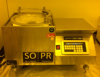
The CEE 100 is a lithography spin coater/developer tool that accepts up to 6-inch wafers and supports programmable multi-step processing.
The Ultratech 1000 Family is a photolithography step-and-repeat 1X steppers family using the Wynne Dyson optical design.