SUSS MicroTec
MA 8 BA 8 Mask

Wafer size
High precision micrometer for wafer alignment adjustment
Performance
Alignment System:[1]
Optics
Backside Optical Alignment[1]
What it is
The SUSS MicroTec MA 8 / BA 8 Mask Aligner is a photolithography mask aligner for backside optical alignment. It supports manual wafer loading and unloading and uses a dedicated mask holder for manual mask loading and unloading.[1]
How it works
The machine uses an ultraviolet mercury lamp and a UV optical path to illuminate the mask and wafer during exposure. It supports proximity, soft contact, and hard contact exposure modes, and the light source position can be adjusted manually.[1]
Where it fits in the process flow
For this model, the specified exposure area is at least 200 mm in diameter, and the alignment stage provides X, Y, and theta motion for positioning during exposure.[1]
Applications
The MA 8 / BA 8 is specified with backside optical alignment, UV400 exposure optics, and resolution down to 0.8 micrometer. The listed proximity mode resolution is 2.5 micrometer at 20 micrometer proximity, and the alignment method is given as TSA accuracy down to 0.5 micrometer.[1]
What do the numbers mean?
Wafer handling2
Optics & imaging7
- Backside Optical Alignment[1]
- Air floating optical table[1]
- High definition & resolution industrial camera[1]
- Optical System:[1]
- UV 400 optical path system[1]
- Equipped with a dedicated mask holder; Manual mask loading / unloading[1]
- Exposure Modes:[1]
Performance1
- Alignment System:[1]
Configuration & options10
Where are the manuals?
Generated from public-source data on file. Enter your email to access — nothing is published; details are routed privately.
Not publicly documented
Field notes
No research found yet — worked with this tool? Share what you know.
Frequently asked questions
What exposure modes does the MA 8 / BA 8 support?
It supports proximity, soft contact, and hard contact exposure modes.[1]
What alignment directions are available on this model?
The alignment stage provides X, Y, and theta adjustment.[1]
What is the specified exposure wavelength range?
The specified wavelength range is UV400, from 350 to 450 nm.[1]
What is the listed exposure-area coverage?
The listed exposure area is at least 200 mm in diameter.[1]
Not publicly documented
The following facts about the MA 8 BA 8 Mask are absent from this record as of this revision. First-hand knowledge or a citation closes a gap; every submission is reviewed before publication.
No publicly documented production dates or lifecycle milestones (introduction, end of production, EOL) for the MA 8 BA 8 Mask are on record.
Answerable by: OEM historical records or a trade-press announcement
No publicly documented variants, configuration options, or revision breakpoints of the MA 8 BA 8 Mask are on record.
Answerable by: an OEM product catalog or an engineer who ordered or specified the tool
The control-system platform and OS era of the MA 8 BA 8 Mask are not on record.
Answerable by: an engineer who operated it or OEM installation records
No publicly documented failure modes or field errata for the MA 8 BA 8 Mask are on record.
Answerable by: a field service engineer, process engineer, or maintenance technician
The process node or technology generation of the MA 8 BA 8 Mask is not on record.
Answerable by: an OEM datasheet or a fab qualification report
No research found yet — worked with this tool? Share what you know.
Sources & citations
Sources (3)Every fact above is drawn from these public sources
- [1]Inventory photo
- [2]Inventory photo
- [3]Inventory photo
Last updated Jul 29, 2026.
Compare with similar tools
View all →Brooks 017-0146-01 is a prealigner manufactured by Brooks.
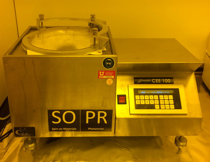
The CEE 100 is a lithography spin coater/developer tool that accepts up to 6-inch wafers and supports programmable multi-step processing.
The Ultratech 1000 Family is a photolithography step-and-repeat 1X steppers family using the Wynne Dyson optical design.