Zeiss
Merlin
Zeiss MERLIN is a scanning electron microscope at CMi. Zeiss MERLIN has a GEMINI II column and a 5-axis motorized stage. Zeiss MERLIN supports a full 4 inch wafer holder.[1]
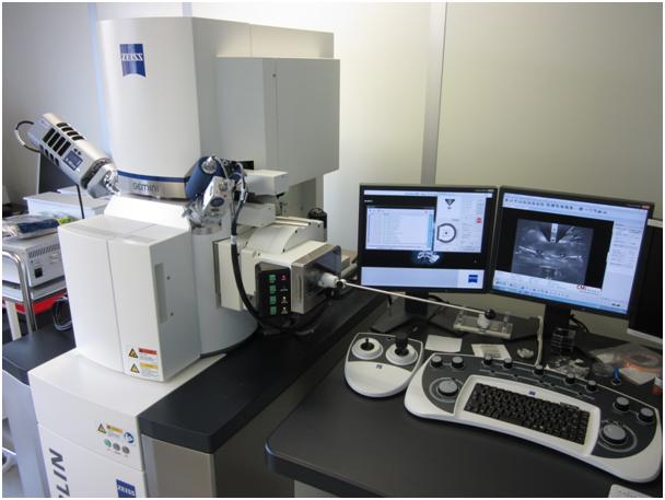
Plate 01VOLK MERLIN on Zeiss microscope
Facundo BWatch on YouTubePlate 02ZEISS MERLIN 3View and SIGMA VP 3View - SBF-SEM/SBEM Workflow Animation
ZEISS MicroscopyWatch on YouTubePlate 03SEM EDX analysis using Zeiss Merlin equipment | Full version
Ahror IsmoiliWatch on YouTube
What it is
General reference — not yet source-verifiedScanning electron microscopes form images by rastering a focused electron beam across a specimen and collecting emitted or reflected signals. In semiconductor and microfabrication work, tools of this class are used for critical inspection, dimensional review, defect observation, materials contrast, and documentation of patterned structures.
How it works
General reference — not yet source-verifiedA scanning electron microscope focuses electrons onto the sample surface and derives contrast from secondary electrons, backscattered electrons, and related signals. Different detector placements emphasize surface detail, topographic contrast, compositional contrast, crystallographic information, or transmission contrast from suitably thin specimens.
Where it fits in the process flow
General reference — not yet source-verifiedIn microfabrication, a scanning electron microscope sits in the characterization and process-control portion of the flow rather than in deposition, lithography, or etch itself. A tool of this class is commonly used after patterning, etching, deposition, cleaning, or sample preparation steps when engineers need image-based confirmation of feature shape, profile, continuity, residue, overlay-related appearance, or defectivity before downstream processing or final analysis.
Applications
General reference — not yet source-verifiedIn fab and lab practice, scanning electron microscopes are applied to patterned lines, contact features, films, particles, fractures, residues, interfaces, and other microstructured surfaces. With suitable detector options, machines in this class can also support elemental analysis, crystallographic mapping, and inspection of insulating or electron-transparent specimens.
- Imaging for process control
- Offline analysis and metrology
- Elemental compositional analysis by EDX
What do the numbers mean?
Power & electrical1
Wafer handling6
Optics & imaging12
Control & software3
Configuration & options7
What replaced it?
Related models
- siblingZeiss Leo 1550— Listed in the same equipment section as Zeiss MERLIN.source[1]
- siblingZeiss CrossBeam 550— The basic training notes differences between the SEM Crossbeam and SEM MERLIN, and state that being fully trained on SEM MERLIN is a prerequisite.source[3]
What does it need to run?
Site utility requirements, footprint, and infrastructure needed to install and operate this tool. Sourced from public records.
- Acceleration voltage0.02–30 kV[2]
Where are the manuals?
Generated from public-source data on file. Enter your email to access — nothing is published; details are routed privately.
Not publicly documented
Field notes
No research found yet — worked with this tool? Share what you know.
Frequently asked questions
What column does the Zeiss Merlin use?
The Zeiss Merlin uses a GEMINI II column with a Schottky field emitter and a combined electrostatic/electromagnetic lens doublet.[1]
What stage does the Zeiss Merlin have?
The stage is motorized with five axes (X, Y, Z, tilt, rotation) and is eucentric, meaning all rotation axes intersect at a single point.[1]
What detectors are available on the Zeiss Merlin?
Three detectors are fitted: an In-Lens detector for high-resolution SE imaging, a HE-SE2 Everhart-Thornley detector for topography, and an EsB with filtering grid for pure material contrast.[1]
Can the Zeiss Merlin perform EDX analysis?
EDX analysis is possible after additional training, and it requires full confirmation of SEM imaging first.[1]
What software controls the Zeiss Merlin?
The microscope is controlled by the ZeissSmartSEM software via a graphical user interface.[1]
Not publicly documented
The following facts about the Merlin are absent from this record as of this revision. First-hand knowledge or a citation closes a gap; every submission is reviewed before publication.
No publicly documented production dates or lifecycle milestones (introduction, end of production, EOL) for the Merlin are on record.
Answerable by: OEM historical records or a trade-press announcement
No publicly documented variants, configuration options, or revision breakpoints of the Merlin are on record.
Answerable by: an OEM product catalog or an engineer who ordered or specified the tool
The control-system platform and OS era of the Merlin are not on record.
Answerable by: an engineer who operated it or OEM installation records
No publicly documented failure modes or field errata for the Merlin are on record.
Answerable by: a field service engineer, process engineer, or maintenance technician
The process node or technology generation of the Merlin is not on record.
Answerable by: an OEM datasheet or a fab qualification report
No research found yet — worked with this tool? Share what you know.
Sources & citations
Sources (4)Every fact above is drawn from these public sources
- [1]epfl.ch — epfl.chepfl.ch
- [2]scopem.ethz.chscopem.ethz.ch
- [3]epfl.chepfl.ch
- [4]Capabilities | UD Nanofabrication Facility — udnf.udel.eduudnf.udel.edu
Last updated Oct 20, 2026.
Compare with similar tools
View all →The Zeiss LEO 1550 is a scanning electron microscope listed in the FIB / SEM / EDX / ProSEM section. The Zeiss LEO 1550 is associated with SEM imaging and sample holders for 4 inch wafers, 6 inch wafers, and 6 inch masks.

The Hitachi SU 8030 FEG-SEM is a field emission gun scanning electron microscope.
The KLA .204 PSL Wafer is an 8-inch NIST-traceable reference wafer compatible with Surfscan 6xy0 and Sp1 particle counters.
KLA .496 PSL Wafer is an 8-inch NIST traceable wafer stated to be capable on Surfscan 6xy0 and SP1.
