Oxford Instruments
Plasmalab 80 Plus
The Oxford Instruments Plasmalab 80 Plus is a compact reactive ion etching (RIE) system with an open-loading design. The Plasmalab 80 Plus supports wafer sizes up to 200mm and includes a 600W RF generator.[1]
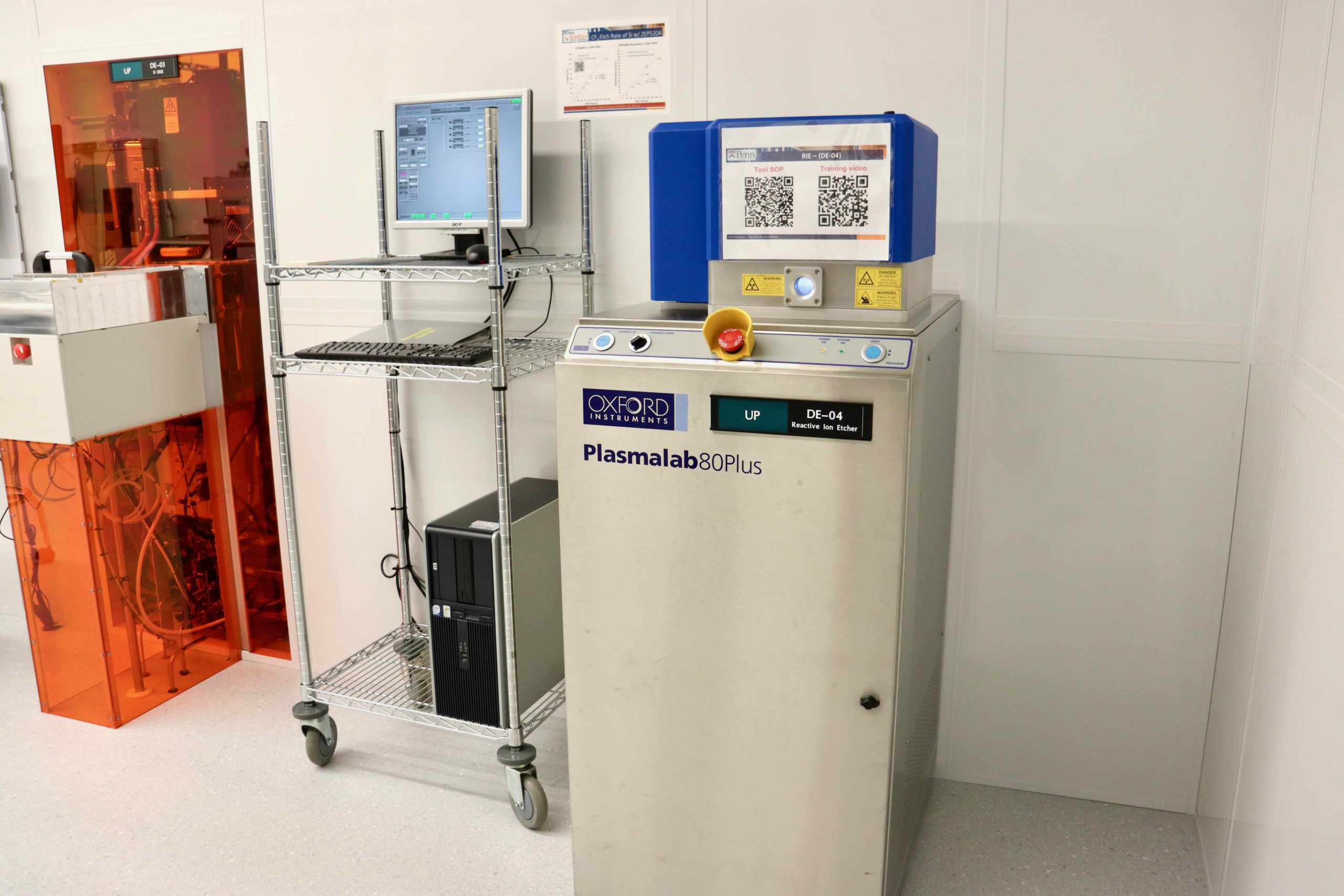
Plate 01Plasmalab 80 Plus RIE
Bid ServicellcWatch on YouTubePlate 02Oxford Instruments Plasmalab 80+ DPCVD semiconductor equipment
SemiStarWatch on YouTubePlate 03Oxford Plasmalab 80 Plus PECVD System (ID# 3908)
ClassOneEngineeringWatch on YouTubePlate 04Oxford PlasmaLab 80+ Video Guide
Yale University CleanroomWatch on YouTubePlate 05Oxford PlasmaLab 80 Plus RIE PECVD Semiconductor equipment ~8 inch
SemiStarWatch on YouTubePlate 06Plasmalab 80 Plus RIE System
Bid ServicellcWatch on YouTubePlate 07Oxford Plasmalab 80 Plus RIE / PE Etcher (ID# 3859)
ClassOneEngineeringWatch on YouTubePlate 08Oxford Plasmalab 80 Plus RIE PE Etcher ID# 3859
TechnolutionsWatch on YouTubePlate 09Video 1 - Oxford Plasmalab 80 Plus RIE System (ID# 3559)
ClassOneEngineeringWatch on YouTubePlate 10Oxford Plasmalab 80 Plus PECVD System (ID# 3864)
ClassOneEngineeringWatch on YouTubePlate 11Video 1 - Oxford Plasmalab 80 Plus RIE System (ID# 3751)
ClassOneEngineeringWatch on YouTubePlate 12Video 1 Oxford Plasmalab 80 Plus RIE System ID# 3751
TechnolutionsWatch on YouTube
What it is
General reference — not yet source-verifiedThe Plasmalab 80 Plus is used as a dry-etch tool in nanofabrication. Reactive ion etch systems remove material from patterned areas of a substrate by combining plasma chemistry with energetic ion bombardment.
How it works
General reference — not yet source-verifiedReactive ion etch tools operate by igniting a plasma from process gases and directing the resulting reactive species and ions toward exposed material. Masked regions remain protected while exposed regions are etched, which makes the class suitable for pattern transfer.
The class generally uses a vacuum process chamber, gas delivery, RF power, and wafer chucking or platen support to control etch rate and uniformity. Open-loading configurations are common in research and pilot production settings because they simplify sample exchange.
Where it fits in the process flow
The Plasmalab 80 Plus fits in the dry-etch segment of microfabrication and nanofabrication flows. The tool is suited to research, prototyping, and low-volume production.[1]
What can it run?
Process applications and technology nodes documented for this tool.
- Reactive ion etching
- Research and development
- Small-scale production
- Prototyping
- Low-volume production
What do the numbers mean?
Power & electrical3
- -Voltage
- 208 VAC, 3 Phase(inventory listing)
Wafer handling6
- Wafer size
- Up to 200mm wafer capable(inventory listing)
Gas & chemistry2
Configuration & options13
- -Process
- PECVD(inventory listing)
- -Equipment component
- Main body(inventory listing)
What replaced it?
Alternatives
Tools documented as functional equivalents — same process step and wafer size, from a different manufacturer. Each equivalence cites its source.
- Plasma-Therm 720/740— Same function class: Etch, 200mmCompare in depthsource[1]
What does it need to run?
Site utility requirements, footprint, and infrastructure needed to install and operate this tool. Sourced from public records.
Where are the manuals?
Publicly hosted documents referencing this tool, linked at their original location. Hosted by the linked institutions — availability may change.
- Oxford-Plasmalab-80plus-Cloey-SOP-Rev-D.pdfSOPasu.edu
- Oxford-Plasmalab-80plus-Rev-C-Floey.pdfDocumentasu.edu
- Oxford PECVD Plasmalab 80Plus Standard Operating ProcedureSOPtamu.edu
Generated from public-source data on file. Enter your email to access — nothing is published; details are routed privately.
Not publicly documented
Field notes
No research found yet — worked with this tool? Share what you know.
Frequently asked questions
Not publicly documented
The following facts about the Plasmalab 80 Plus are absent from this record as of this revision. First-hand knowledge or a citation closes a gap; every submission is reviewed before publication.
No publicly documented production dates or lifecycle milestones (introduction, end of production, EOL) for the Plasmalab 80 Plus are on record.
Answerable by: OEM historical records or a trade-press announcement
No publicly documented variants, configuration options, or revision breakpoints of the Plasmalab 80 Plus are on record.
Answerable by: an OEM product catalog or an engineer who ordered or specified the tool
The control-system platform and OS era of the Plasmalab 80 Plus are not on record.
Answerable by: an engineer who operated it or OEM installation records
No publicly documented failure modes or field errata for the Plasmalab 80 Plus are on record.
Answerable by: a field service engineer, process engineer, or maintenance technician
The process node or technology generation of the Plasmalab 80 Plus is not on record.
Answerable by: an OEM datasheet or a fab qualification report
No research found yet — worked with this tool? Share what you know.
Sources & citations
Sources (11)Every fact above is drawn from these public sources
- [1]nano.upenn.edu — nano.upenn.edunano.upenn.edu
- [2]Inventory photo
- [3]Inventory photo
- [4]Inventory photo
- [5]Inventory photo
- [6]cores.research.asu.edu — cores.research.asu.educores.research.asu.edu
- [7]Oxford Plasmalab80Plus (PECVD) - AggieFab Nanofabrication Facility — aggiefab.tamu.eduaggiefab.tamu.edu
- [8]Physical Vapor Deposition — nanolab.berkeley.edunanolab.berkeley.edu
- [9]University-of-Utah-94-721002-System-Manual — nanofab.utah.edunanofab.utah.edu
- [10]Oxford Plasmalab 80 Plus | UCLA Nanolab — nanolab.ucla.edunanolab.ucla.edu
- [11]PECVD System Manual - Maryland University 94-219896 .pdf — nanocenter.umd.edunanocenter.umd.edu
Last updated Oct 8, 2026.
Compare with similar tools
View all →The Plasma Therm 720/740 is a dual-chamber RIE loadlocked system with chlorine- and fluorine-based chemistry.

Tegal 980 ACS is a plasma etch system series described as serving the 200mm fab line.
The Oxford Instruments PlasmaPro NGP80 is a modular, benchtop-scale plasma processing platform for precision thin-film deposition and reactive ion etching (RIE).
The Memsstar Orbis Alpha Oxide Etch System is a small-footprint, self-contained oxide etch system that uses hydrogen fluoride etchants.