Wafer size
200mm
Looking for practical guidance on 200mm? The reference remains the primary source; requests are private, the network is growing, and a relevant match is not guaranteed.
67 entries
- R50Filmetrics
The Filmetrics R50 – 200 – 4PP is a metrology tool configured by default for metallic layers and sample thicknesses of 525 µm ± 25 µm.
CategoryMetrology & InspectionWafer200mm - 720/740Plasma-Therm
The Plasma Therm 720/740 is a dual-chamber RIE loadlocked system with chlorine- and fluorine-based chemistry.
CategoryEtchWafer200mm - LabSpin6 / 8SUSS MicroTec
The LabSpin6 / 8 is a manual coating and developing system for substrates up to 200 mm, capable of spin coating and puddle developing.
Wafer200mm - HP8 / CP8 / VP8SUSS MicroTec
The HP8, CP8, and VP8 are manual coating and developing systems from SUSS MicroTec, supporting wafers up to 200 mm and offering baking, cooling, and vapor priming capabilities.
Wafer200mm - Plasmalab 80 PlusOxford Instruments
Oxford Instruments Plasmalab 80+ is a compact open-loading reactive ion etch system for R&D or small-scale production.
CategoryEtchWafer200mm - DektakVeeco
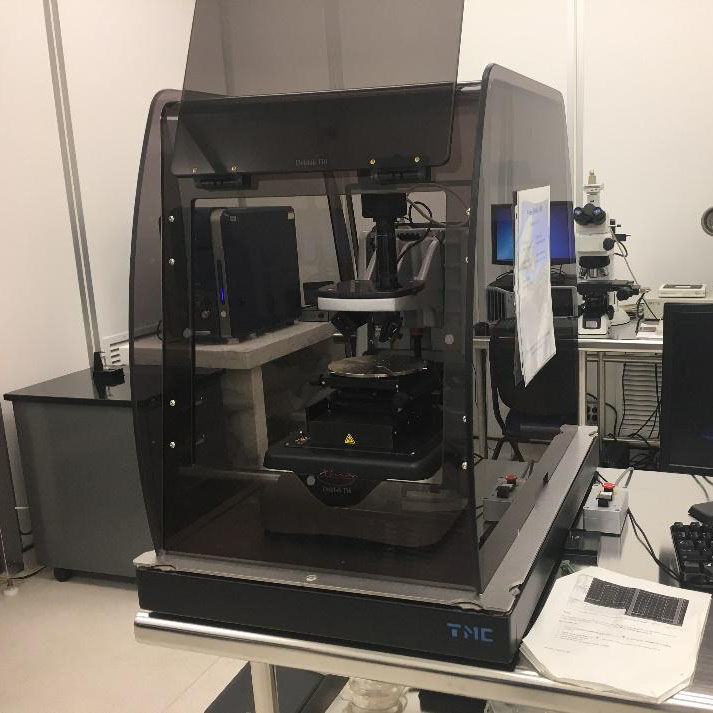
Veeco Dektak 150 is a stylus-based surface profiler used for measuring surface topography and thin film step heights.
CategoryMetrology & InspectionWafer200mm - , Vistec INS 3000Leica
Leica Vistec INS 3000 is an optical defect review station with bright field light source, DIC DUV light source, UV and DUV camera, and a single 150/200 mm wafer loadport.
Wafer200mm - NSR 2205 i 14 E 2 i-LineNikon
Nikon NSR 2205 i 14 E 2 is an i-line stepper.
CategoryLithographyWafer200mm - 3200Tegal
The Tegal 3200 SE is an advanced cluster platform for 3D IC and MEMS applications that can be configured with up to 3 process modules.
Categoryadvanced cluster platformWafer200mm - 200CBXCEE
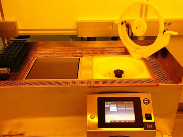
The CEE 200CBX is a precision coat-bake system described as a track-quality spin coater with a high-uniformity bake plate.
Categoryspin coaterWafer200mm - Orbis Alphamemsstar
The Memsstar Orbis Alpha Oxide Etch System is a small-footprint, self-contained oxide etch system that uses hydrogen fluoride etchants.
CategoryEtchWafer200mm - WS-650-8BLaurell
The Laurell WS-650-8B is a spin coater in the 650 Series with a maximum substrate size of ø200mm (7" x 7") and a maximum speed of 12,000 rpm.
CategoryResist ProcessingWafer200mm - H6-8 BLaurell
The Laurell H6-8 B is a spin coater in the 650-series with a maximum substrate size of 200mm (7" x 7"), a maximum speed of 12000 rpm, and tabletop, in-deck, or on-deck mounting options.
CategoryResist ProcessingWafer200mm - EDC-HL-8 BLaurell
Laurell EDC-HL-8 B is an EDC System 650-series spin coater with a maximum substrate size of 200mm (7" x 7").
CategoryResist ProcessingWafer200mm - 4200Tegal
The Tegal 4200 SE is an advanced cluster platform for 3D IC and MEMS applications.
Categorycluster platformWafer200mm - Scientific FEI NanoLab 1200 AT FIBThermo Fisher
The Thermo Fisher Scientific / FEI NanoLab 1200 AT FIB is a focused ion beam system with an integrated Electron column and supporting inspection, wafer handling, and gas delivery components.
Wafer200mm - c2LSPTS
SPTS lists the c2L as a 200mm tool in its Equipment Training course offerings.
CategoryOperation and MaintenanceWafer200mm - E 2000 Epitaxial ReactorASM
The ASM E 2000 is a radiantly heated, single-wafer epitaxial reactor for chemical vapor deposition of doped or undoped silicon layers on wafers up to 200 mm (8 inches).
CategoryDepositionWafer200mm - RC2J.A. Woollam
The J.A. Woollam RC2 is a spectroscopic ellipsometer used to measure thin-film thickness and refractive indices.
CategoryPrecision OpticsWafer200mm - EDC-HL-8Laurell
The Laurell EDC-HL-8 B is a compact EDC spin processor that accommodates up to 200 mm wafers and 7 in × 7 in substrates.
CategorySpin coaterWafer200mm - BA8 Gen4 ProSUSS MicroTec
The SUSS MicroTec BA8 Gen4 Pro is a semi-automated mask alignment and wafer bonding system for 200 mm wafers, with capabilities including exposure, UV bonding, fusion bonding, imprinting, and selective plasma activation.
CategoryLithographyWafer200mm - 200 Bake PlateCEE
The CEE 200 Bake Plate is a bake plate for up to 200mm wafers with Internal OS software and 208V power.
CategoryThermal / DiffusionWafer200mm - SS W 80 A-ARSCREEN
The SCREEN / DNS SS W 80 A-AR is a scrubber with 8 inch wafer size support.
CategoryWet Processing / CleanWafer200mm - AST-3100Despatch
The Despatch AST-3100 is an automated polyimide curing tool designed for 200mm and 300mm wafers.
CategoryAutomated polyimide curing toolWafer200mm - 980Tegal
Tegal 980 ACS is a plasma etch system series described as serving the 200mm fab line.
CategoryEtchWafer200mm - UF 200 SAccretech
The Accretech / TSK UF 200 S is a prober for 8-inch wafers, with sources also stating it was configured for 8-inch (200mm) operation.
CategoryTest & ProbeWafer200mm - 850 LT SOI Fusion WaferEV Group
The EV Group 850 LT SOI Fusion Wafer Bonder is a fully automatic wafer bonder configured for 8-inch/200mm wafers.
CategoryPackaging & BondingWafer200mm - Gemini Automated Production WaferEV Group
The EVG Gemini Automated Production Wafer Bonder is a wafer bonder with face-to-face alignment and automation features, supporting wafers up to 8"/200mm.
CategoryPackaging & BondingWafer200mm - PlasmaPro80Oxford Instruments
Oxford Instruments PlasmaPro80 is an RIE dry etcher used for hBN, SiGe, graphite, and graphene etching.
CategoryEtchWafer200mm - Z3D-7000Zygo
The ZYGO Z3D-7000 is a non-contact, optical metrology system for semiconductor wafers that accommodates 200 mm and 300 mm wafer sizes.
CategoryMetrology & InspectionWafer200mm - sem2Zeiss
Zeiss 200 mm Scanning Electron Microscope.
CategoryMetrology & InspectionWafer200mm - BSG-200AJA
The AJA BSG-200 Series Substrate Holder is a backside-gas-cooled rotating substrate holder for wafers or similar planar substrates up to 200 mm in diameter.
CategorySubstrate holderWafer200mm - EVG40EV Group
EVG40 is an EV Group top-to-bottom side alignment accuracy measurement inspection system for non-destructive measurement of repeatable alignment accuracy.
CategoryMetrology & InspectionWafer200mm - 4300 S SRDSemitool
The Semitool 4300 S SRD is a spin rinse dryer with a single-stack configuration and 200mm wafer particle specification.
CategoryCMPWafer200mm - WS-650-8Laurell
The Laurell WS-650-8B is a compact 650-series spin coater with a maximum rotational speed of 12,000 RPM and support for wafers up to 200 mm.
CategorySpin coaterWafer200mm - 8-2P-CPYES
The YES 8-2P-CP is a manual-load high-temperature cure oven in the PB Series, specified for 200 mm wafers.
CategoryThermal / DiffusionWafer200mm - Archer 10 XT OverlayKLA
The KLA Archer 10 XT Overlay System is a 200mm overlay metrology system with refurbishment-upgraded components and software version 5.6.
CategoryMetrology & InspectionWafer200mm - MA200 Gen3SUSS MicroTec
The SUSS MicroTec MA200 Gen3 is a fully automated mask aligner for high-volume lithography on wafers and square substrates up to 200 mm.
CategoryLithographyWafer200mm - MVD300SPTS
The SPTS MVD300 is a Molecular Vapor Deposition system designed for high-performance, flexible, reliable high-volume manufacturing applications.
CategoryDepositionWafer200mm - PAS 5500ASML
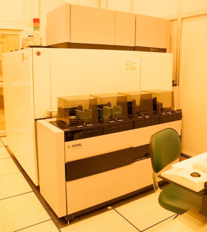
The ASML PAS 5500/275D is a high-throughput i-line stepper with 5X reduction, 365 nm exposure, and automated wafer handling for substrates up to 200 mm diameter.
CategoryLithographyWafer200mmNode280 nmLegacy - F54Filmetrics
The Filmetrics F54 is a spectroscopic ellipsometer for measuring thin-film thickness and refractive index.
CategoryPrecision OpticsWafer200mm - P-15KLA
The KLA Tencor P-15 is a profilometer with a 200 mm sample table with vacuum.
CategoryMetrology & InspectionWafer200mm - 501EV GroupCategoryDicing & GrindingWafer200mm
- EDC-650-8Laurell
The Laurell EDC-650-8 is a station-mounted spin processor that accommodates up to 200 mm wafers and 7 in x 7 in substrates.
CategorySpin processorWafer200mm - MVD100ESPTS
The SPTS MVD100E is a Molecular Vapor Deposition system designated for R&D or pilot manufacturing.
CategoryDepositionWafer200mm - EG4Electroglas
Electroglas EG4|200 is a wafer prober for 200mm wafer applications, and the EG4|200e is a related variant described for ultra-low-noise probing.
CategoryTest & ProbeWafer200mm - NGP80Oxford Instruments
The Oxford Instruments PlasmaPro NGP80 is a modular, benchtop-scale plasma processing platform for precision thin-film deposition and reactive ion etching (RIE).
CategoryEtchWafer200mm - plasmapro-ngp80-rieOxford Instruments
The PlasmaPro NGP80 RIE is an Oxford Instruments reactive ion etching system used for processes such as SiO2 hard mask etching with CHF3/Ar plasma at 20°C.
CategoryEtchWafer200mm - H6-8Laurell
The Laurell H6-8 is a 650-series HL spin coater that accommodates up to 200mm wafers and 7" × 7" substrates and has a maximum rotational speed of 12,000 RPM.
CategorySpin coaterWafer200mm - AS200GCA
The GCA AutoStep 200 DSW (also known as AS200) is a 5X reduction i-line wafer stepper designed for up to 200mm wafers.
CategoryLithographyWafer200mm - RS50Filmetrics
The Filmetrics RS50 is a 4-point probe mapping system for sheet resistance measurement.
CategoryTest & ProbeWafer200mm - P-2KLA
The KLA Tencor P-2 is a profilometer with a 200 mm sample table with vacuum and a 3D scan option.
CategoryMetrology & InspectionWafer200mm - NV 8200Axcelis
General referenceThe Axcelis NV 8200 is an ion implantation system used in semiconductor manufacturing to introduce dopant atoms into a substrate.
CategoryIon ImplantationWafer200mm - CV108YES
The YES CV108 is a single-wafer downstream plasma stripper/descummer for removing photoresist, polyimide, and B.C.B. coatings.
CategorySingle-wafer downstream plasma stripper/descummerWafer200mm - TS2000-IFEMPI
The MPI TS2000-IFE is a 200-mm automated probe station with micron precision used in a terahertz small-signal probe station configuration.
CategoryTest & ProbeWafer200mm - XB8SUSS MicroTec
The SUSS MicroTec XB8 is a semi-automated wafer bonding system for substrates up to 200 mm, supporting high-force wafer bonding.
CategoryPackaging & BondingWafer200mm - EDC-650-8BLaurell
The Laurell EDC-650-8B is an EDC System 650 Series spin coater with a maximum substrate size of 200mm (7" x 7").
CategoryResist ProcessingWafer200mm - WS-650-8 BLaurell
The Laurell WS-650-8 B is a 650-series spin coater with a maximum substrate size of 200mm (7" x 7") and a maximum speed of 12000 rpm.
CategoryResist ProcessingWafer200mm - EDC-650-8 BLaurell
The Laurell EDC-650-8 B is an EDC System 650-series spin coater with a maximum substrate size of ø 200mm (7" × 7") and a maximum speed of 12000 rpm.
CategoryResist ProcessingWafer200mm - dad3240-dicing-sawDisco
The Disco DFL7340 stealth dicing system is used for dicing silicon wafers and is dedicated to Si wafers only.
CategoryPackaging & BondingWafer200mm