Zeiss
sem2
Provisional entry — research in progress
This page was generated automatically from cited public sources and hasn't completed the full research pass yet. Every specification shown carries its source; more detail is added as research completes.

What it is
The Zeiss sem2 is a scanning electron microscope used for metrology and inspection.[2]
How it works
General reference — not yet source-verifiedA scanning electron microscope scans a focused electron beam across a sample surface and detects signals generated by the beam-sample interaction to form an image.
Metrology and inspection use of a scanning electron microscope centers on visualizing small features, checking pattern fidelity, and examining surface condition at high magnification.
Where it fits in the process flow
General reference — not yet source-verifiedScanning electron microscopy is typically used after fabrication steps that create or modify surface features, when a process engineer needs dimensional inspection or defect review before further processing.
Applications
The Zeiss sem2 supports device characterization tasks that include surface topography analysis and scanning electron microscopy.[2]
The Zeiss sem2 is used for optical microscopy and imaging tasks in the metrology area, including inspection of fine structural detail.[2]
- Scanning electron microscopy
What do the numbers mean?
Wafer handling1
Configuration & options5
Where are the manuals?
Generated from public-source data on file. Enter your email to access — nothing is published; details are routed privately.
Not publicly documented
Field notes
No research found yet — worked with this tool? Share what you know.
Frequently asked questions
What category of instrument is the Zeiss sem2?
The Zeiss sem2 is a scanning electron microscope.[2]
Where is the Zeiss sem2 used in the laboratory workflow?
The Zeiss sem2 is part of the metrology and inspection area, which supports device characterization.[2]
What kind of measurements does the metrology area support around the Zeiss sem2?
The metrology area supports surface topography analysis, film thickness and optical property measurements, structural and compositional analysis, high resolution optical microscopy, and scanning electron microscopy.[2]
Not publicly documented
The following facts about the sem2 are absent from this record as of this revision. First-hand knowledge or a citation closes a gap; every submission is reviewed before publication.
No publicly documented production dates or lifecycle milestones (introduction, end of production, EOL) for the sem2 are on record.
Answerable by: OEM historical records or a trade-press announcement
No publicly documented variants, configuration options, or revision breakpoints of the sem2 are on record.
Answerable by: an OEM product catalog or an engineer who ordered or specified the tool
The control-system platform and OS era of the sem2 are not on record.
Answerable by: an engineer who operated it or OEM installation records
No publicly documented failure modes or field errata for the sem2 are on record.
Answerable by: a field service engineer, process engineer, or maintenance technician
The process node or technology generation of the sem2 is not on record.
Answerable by: an OEM datasheet or a fab qualification report
No research found yet — worked with this tool? Share what you know.
Sources & citations
Sources (3)Every fact above is drawn from these public sources
- [1]nanolab.berkeley.edu — nanolab.berkeley.edunanolab.berkeley.edu
- [2]Metrology — nanolab.berkeley.edunanolab.berkeley.edu
- [3]Capabilities — nanolab.berkeley.edunanolab.berkeley.edu
Last updated Oct 4, 2026.
Compare with similar tools
View all →
The KLA Archer 10 XT Overlay System is a 200mm overlay metrology system with refurbishment-upgraded components and software version 5.6.
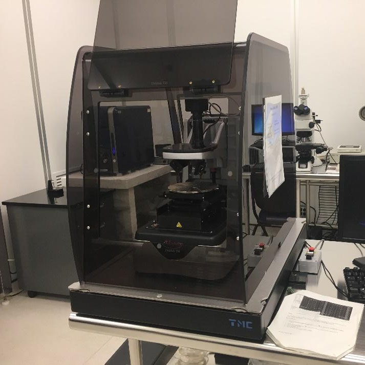
Veeco Dektak 150 is a stylus-based surface profiler used for measuring surface topography and thin film step heights.
EVG40 is an EV Group top-to-bottom side alignment accuracy measurement inspection system for non-destructive measurement of repeatable alignment accuracy.
The KLA Tencor P-15 is a profilometer with a 200 mm sample table with vacuum.