Veeco
Dektak
The Veeco Dektak 150 is a stylus-based surface profiler used for measuring surface topography and thin film step heights. The Dektak 150 accommodates samples up to 200 mm in diameter and up to 90 mm thick. The Dektak 150 can measure steps in the nanometer range and profile surface topography, waviness, and surface roughness.[1]
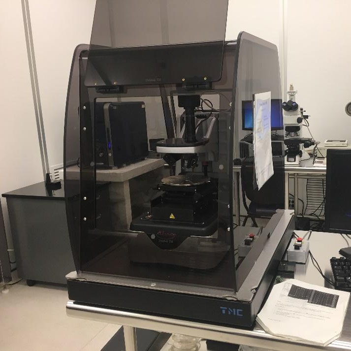
Plate 01Veeco Dektak 150 Surface Profiler
Bid ServicellcWatch on YouTubePlate 02Veeco Dektak 150 Profiler #63162
Bid ServicellcWatch on YouTubePlate 03Veeco Dektak 150 Profiler #61255
Bid ServicellcWatch on YouTubePlate 04Veeco Dektak 3 Profiler #61949
Bid ServicellcWatch on YouTubePlate 05Veeco Dektak 150 Inv# 64,292
Bid ServicellcWatch on YouTubePlate 06Veeco Dektak 3 Surface Profiler No. 63
Bid ServicellcWatch on YouTubePlate 07Veeco DEKTAK 150 Profilometer #60749
Bid ServicellcWatch on YouTubePlate 08Veeco Dektak 8 refurbished demo, Corenex
Fan BensonWatch on YouTubePlate 09The Veeco Dektak 150 Surface Profilometer
azonanoWatch on YouTubePlate 10Veeco Dektak 150 Profiler #59579
Bid ServicellcWatch on YouTubePlate 11Dektak Veeco 8 Stylus Profilometry
corematerialsWatch on YouTube
What it is
The Veeco Dektak is a stylus surface profiler used for metrology and inspection. It is a scanning instrument for measuring surface topography and thin film step heights.[1]
How it works
The Dektak 150 uses stylus-based scanning and includes manual sample positioning and leveling features. It is intended for profiling surfaces and measuring thin film step heights in the nanometer range.[1]
Where it fits in the process flow
The Dektak 150 is used for surface topography and waviness measurements, as well as surface roughness evaluation. It is also used for thin and thick film step height measurement.[1]
Applications
The instrument is used to measure surface topography, waviness, and roughness, and to determine step heights on thin and thick films.[1]
It is suited to samples up to 200 millimeters in diameter and up to 90 millimeters thick, with long scan capability of 55 millimeters.[1]
- Measuring surface topography
- Measuring thin film step heights
- Measuring surface roughness
- Measuring waviness
What do the numbers mean?
Control & software1
Configuration & options18
- Purpose
- Stylus-based scanning system for measuring surface topography and thin film step heights[1]
What replaced it?
Alternatives
Tools documented as functional equivalents — same process step and wafer size, from a different manufacturer. Each equivalence cites its source.
- KLA P-2— Same function class: Metrology & Inspection, 200mmCompare in depthsource[2]
- KLA P-15— Same function class: Metrology & Inspection, 200mmCompare in depthsource[2]
Where are the manuals?
Publicly hosted documents referencing this tool, linked at their original location. Hosted by the linked institutions — availability may change.
- PROF2_OperatingProcedure.pdfDocumentduke.edu
Generated from public-source data on file. Enter your email to access — nothing is published; details are routed privately.
Not publicly documented
Field notes
No research found yet — worked with this tool? Share what you know.
Frequently asked questions
Not publicly documented
The following facts about the Dektak are absent from this record as of this revision. First-hand knowledge or a citation closes a gap; every submission is reviewed before publication.
No publicly documented production dates or lifecycle milestones (introduction, end of production, EOL) for the Dektak are on record.
Answerable by: OEM historical records or a trade-press announcement
No publicly documented variants, configuration options, or revision breakpoints of the Dektak are on record.
Answerable by: an OEM product catalog or an engineer who ordered or specified the tool
The control-system platform and OS era of the Dektak are not on record.
Answerable by: an engineer who operated it or OEM installation records
No publicly documented failure modes or field errata for the Dektak are on record.
Answerable by: a field service engineer, process engineer, or maintenance technician
The process node or technology generation of the Dektak is not on record.
Answerable by: an OEM datasheet or a fab qualification report
No research found yet — worked with this tool? Share what you know.
Sources & citations
Sources (7)Every fact above is drawn from these public sources
- [1]uwaterloo.ca — uwaterloo.cauwaterloo.ca
- [2]egr.vcu.edu — egr.vcu.eduegr.vcu.edu
- [3]Get started | NanoFab | Core Facilities | ASU — cores.research.asu.educores.research.asu.edu
- [4]Fab.nano Equipment Rates External March 2026 — nanousers.mit.edunanousers.mit.edu
- [5]PROF2_OperatingProcedure.pdf — smif.pratt.duke.edusmif.pratt.duke.edu
- [6]Veeco Dektak 150 Surface Profiler | UCLA Nanolab — nanolab.ucla.edunanolab.ucla.edu
- [7]Request Info — veeco.com (Jan 7, 2004)web.archive.org
Last updated Sep 21, 2026.
Compare with similar tools
View all →The KLA Tencor P-15 is a profilometer with a 200 mm sample table with vacuum.
The KLA Tencor P-2 is a profilometer with a 200 mm sample table with vacuum and a 3D scan option.

The KLA Archer 10 XT Overlay System is a 200mm overlay metrology system with refurbishment-upgraded components and software version 5.6.
EVG40 is an EV Group top-to-bottom side alignment accuracy measurement inspection system for non-destructive measurement of repeatable alignment accuracy.