KLA
P-15
The KLA P-15 is a profilometer. The KLA P-15 measures step height, roughness, waviness, and other surface characteristics. The KLA P-15 has a 200 mm sample table with vacuum.[1][2]
Plate 01KLA Tencor P 15 Profiler #62240
Bid ServicellcWatch on YouTubePlate 02KLA Tencor P-15 Wafer Surface Profilometer System w/ Computer USED (7289)R
Anacapa EquipmentWatch on YouTubePlate 03Kel-Tec P15: The Smallest, Lightest Doublestack 9mm
TFB TVWatch on YouTubePlate 04What’s your opinion on the Kel-Tec P15 9mm?
Duke's Sport ShopWatch on YouTubePlate 05Refublished KLA Tencor P15 中古段差測定器
株式会社ナノ・ソルテックWatch on YouTubePlate 06What Do You Guys Think About The New Budget Friendly Kel-Tec P15? Cop or Drop? #Viral #Fyp #Ytshorts
Payso SafariWatch on YouTube
Wafer size
200mm
Vacuum
200 mm sample table with vacuum[1]
What it is
The KLA P-15 is a profilometer used in metrology and inspection.[3]
The KLA Tencor P-15 Profilometer uses a 200 mm sample table with vacuum hold-down.[1]
How it works
Where it fits in the process flow
The KLA Tencor P-15 is intended for sample sizes down to a minimum sample length of 25 mm, with smaller samples requiring staff review.[1]
Applications
What do the numbers mean?
Vacuum & pumping1
Wafer handling1
Control & software3
Dimensions & facilities1
- Measurement capabilities
- Measures roughness, waviness, step height, and other surface characteristics[2]
Configuration & options4
What replaced it?
Alternatives
Tools documented as functional equivalents — same process step and wafer size, from a different manufacturer. Each equivalence cites its source.
- Veeco Dektak— Same function class: Metrology & Inspection, 200mmCompare in depthsource[4]
What does it need to run?
Site utility requirements, footprint, and infrastructure needed to install and operate this tool. Sourced from public records.
- Sample table200 mm sample table with vacuum[1]
Where are the manuals?
Generated from public-source data on file. Enter your email to access — nothing is published; details are routed privately.
Not publicly documented
Field notes
No research found yet — worked with this tool? Share what you know.
Frequently asked questions
What does the KLA P-15 measure?
The KLA Tencor P-15 measures surface morphology and film thickness. The KLA Tencor P-15 also measures roughness, waviness, step height, and other surface characteristics.[6][2]
What sample size does the KLA P-15 support?
The KLA Tencor P-15 uses a 200 mm sample table with vacuum hold-down. The KLA Tencor P-15 has a minimum sample length of 25 mm, and staff review is requested for smaller samples.[1]
What range of step heights can the KLA P-15 measure?
The KLA Tencor P-15 measures steps from 100 Å to 300 µm.[1]
Which wafer diameters can the KLA P-15 accept?
The KLA-Tencor P15 can accept wafers with diameters of 50 mm, 75 mm, 100 mm, and 150 mm.[5]
Not publicly documented
The following facts about the P-15 are absent from this record as of this revision. First-hand knowledge or a citation closes a gap; every submission is reviewed before publication.
No publicly documented production dates or lifecycle milestones (introduction, end of production, EOL) for the P-15 are on record.
Answerable by: OEM historical records or a trade-press announcement
No publicly documented variants, configuration options, or revision breakpoints of the P-15 are on record.
Answerable by: an OEM product catalog or an engineer who ordered or specified the tool
The control-system platform and OS era of the P-15 are not on record.
Answerable by: an engineer who operated it or OEM installation records
No publicly documented failure modes or field errata for the P-15 are on record.
Answerable by: a field service engineer, process engineer, or maintenance technician
The process node or technology generation of the P-15 is not on record.
Answerable by: an OEM datasheet or a fab qualification report
No research found yet — worked with this tool? Share what you know.
Sources & citations
Sources (6)Every fact above is drawn from these public sources
- [1]nanofab.ece.cmu.edu — nanofab.ece.cmu.edunanofab.ece.cmu.edu
- [2]classoneequipment.com — classoneequipment.comclassoneequipment.com
- [3]nanofab.ece.cmu.edu — nanofab.ece.cmu.edunanofab.ece.cmu.edu
- [4]egr.vcu.eduegr.vcu.edu
- [5]KLA-Tencor P-15 stylus profilometer — mems-exchange.orgmems-exchange.org
- [6]KLA-Tencor P15 | Office of Research and Partnerships (ORP) Core Facilities — cores.arizona.educores.arizona.edu
Last updated Oct 9, 2026.
Compare with similar tools
View all →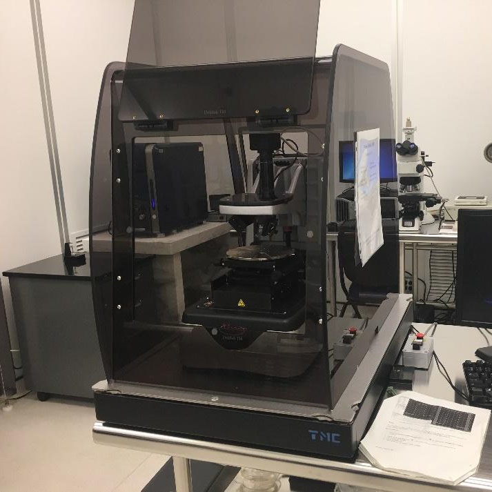
Veeco Dektak 150 is a stylus-based surface profiler used for measuring surface topography and thin film step heights.

The KLA Archer 10 XT Overlay System is a 200mm overlay metrology system with refurbishment-upgraded components and software version 5.6.
EVG40 is an EV Group top-to-bottom side alignment accuracy measurement inspection system for non-destructive measurement of repeatable alignment accuracy.
The KLA Tencor P-2 is a profilometer with a 200 mm sample table with vacuum and a 3D scan option.