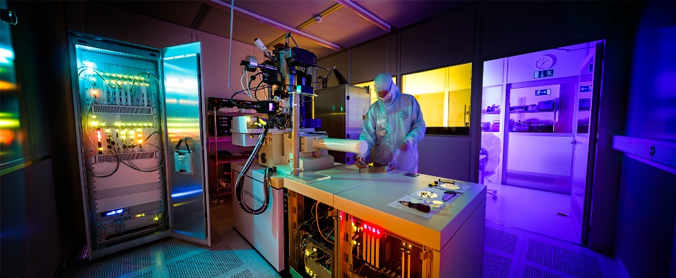
Karl Suss
MA6
The Karl Suss MA6 is a semi-automated mask aligner for photolithography. The MA6 supports top-side and bottom-side alignment. The MA6 achieves resolution down to 0.6 µm under optimum vacuum conditions.[1][2]

Plate 01Karl Suss MA6 Mask Aligner - Standard Operating Procedures
InrfucirvineWatch on YouTubePlate 02Exposure using contact aligner (Suss MA6)
Micro System Integration Center(uSIC), Tohoku UnivWatch on YouTubePlate 03Karl Suss MA6 Mask Aligner Part 2
Bid ServicellcWatch on YouTubePlate 04Karl Suss MA6 BSA Mask Aligner
ClassOneVideosWatch on YouTubePlate 05Video 1 of 2 - Karl Suss MA6/BA6 Mask Aligner (ID# 3733)
ClassOneEngineeringWatch on YouTubePlate 06Aligner: MA6 - 2 Part I (Operation) at DTU's cleanroom facility - Nanolab
DTU NanolabWatch on YouTubePlate 07Karl Suss MA6 - Backside and Topside Alignment
InrfucirvineWatch on YouTubePlate 08Karl Suss MA6 Mask Aligner
Bid ServicellcWatch on YouTubePlate 09Karl Suss MA6 Mask Aligner 7-26-13
Bid ServicellcWatch on YouTube
Wafer size
150mm
Node / era
1 micron and better; 0.6 µm under optimum conditions in vacuum mode
Vacuum
0.6 µm (optimum conditions)[1]
Performance
0.5 µm[1]
Optics
Channel 1 (405 nm) and Channel 2 (365 nm)[1]
What it is
The Karl Suss MA6 is a photolithography mask aligner used to transfer patterns from photomasks onto photoresist-coated substrates. It is a high resolution semi-automated tool intended for research and development and small volume production.[1]
How it works
The tool uses ultraviolet exposure to transfer mask patterns to resist on the substrate. Its alignment system includes a splitfield microscope for fiducial alignment, storage and automatic movement between reference points, and bottom-side alignment for aligning backside features to the photomask.[1]
Applications
The MA6 is used in semiconductor research, MEMS development, microfluidics, and optical component production.[1]
- semiconductor research
- MEMS-development
- microfluidics
- optical component production
What do the numbers mean?
Vacuum & pumping6
Wafer handling8
Optics & imaging10
Performance5
- Alignment features
- Splitfield microscope with storage and automatic movement between reference points; Bottom-Side Alignment (BSA); Wedge Error Compensation (WEC)[1]
Configuration & options2
Vintage & configurations
Documented models & variants
| Designation | Generation | Vintage | Changes | Source |
|---|---|---|---|---|
| MA4 | — | — | The MA6 and MA4 Mask Aligners use UV light to transfer patterns from photomasks onto substrates coated with photoresist; the MA6 is listed with wafers up to 6 inches while the MA4 is listed with wafers up to 4 inches. | ece.utoronto.ca[5] |
| MA6/BA6 | — | — | Front and backside alignment capabilities are stated for the MA6/BA6 mask aligners. | louisville.edu[6] |
What replaced it?
Alternatives
Tools documented as functional equivalents — same process step and wafer size, from a different manufacturer. Each equivalence cites its source.
- SUSS MicroTec MA / BA Gen4 Pro Series— Same function class: Lithography, 150mmCompare in depthsource[1]
- SUSS MicroTec MA100 / 150e Gen2— Same function class: Lithography, 150mmCompare in depthsource[1]
What does it need to run?
Site utility requirements, footprint, and infrastructure needed to install and operate this tool. Sourced from public records.
- Resolution0.6 µm under optimum conditions in vacuum mode[1]
- Exposure modesproximity, soft contact, hard contact, and vacuum[1]
- Exposure modesProximity, soft contact, hard contact, vacuum[1]
- Resolution (vacuum mode)0.6 µm (optimum conditions)[1]
- Resolution (optimum vacuum mode)0.6 µm[1]
- Exposure methodsflood, proximity, soft contact, hard contact, low vacuum, vacuum[2]
Where are the manuals?
Publicly hosted documents referencing this tool, linked at their original location. Hosted by the linked institutions — availability may change.
- User ManualManualepfl.ch
- Photomask Layout and Generation Guide Rev1.pdfDocumentduke.edu
- PHOTO2 MA6 Top Side Align Operating Procedure Rev 5.pdfDocumentduke.edu
- ManualManualuic.edu
Generated from public-source data on file. Enter your email to access — nothing is published; details are routed privately.
Not publicly documented
Field notes
No research found yet — worked with this tool? Share what you know.
Frequently asked questions
What substrate sizes can the MA6 handle?
It can handle irregularly shaped substrates ranging from 5 x 5 mm dies to wafers up to 150 mm.[1]
What illumination wavelengths are specified?
The tool uses a broadband Hg lamp with channel 1 at 405 nm and channel 2 at 365 nm.[1]
What applications is it used for?
It is used in semiconductor research, MEMS development, microfluidics, and optical component production.[1]
Not publicly documented
The following facts about the MA6 are absent from this record as of this revision. First-hand knowledge or a citation closes a gap; every submission is reviewed before publication.
No publicly documented production dates or lifecycle milestones (introduction, end of production, EOL) for the MA6 are on record.
Answerable by: OEM historical records or a trade-press announcement
The control-system platform and OS era of the MA6 are not on record.
Answerable by: an engineer who operated it or OEM installation records
No publicly documented failure modes or field errata for the MA6 are on record.
Answerable by: a field service engineer, process engineer, or maintenance technician
No publicly documented compatible parts, consumables, or accessories for the MA6 are on record.
Answerable by: an OEM parts catalog or a service engineer
No research found yet — worked with this tool? Share what you know.
Sources & citations
Sources (13)Every fact above is drawn from these public sources
- [1]ncf.uic.edu — ncf.uic.eduncf.uic.edu
- [2]nanolab.ucla.edu — nanolab.ucla.edunanolab.ucla.edu
- [3]Inventory photo
- [4]Inventory photo
- [5]ece.utoronto.ca — ece.utoronto.caece.utoronto.ca
- [6]louisville.edu — louisville.edulouisville.edu
- [7]Equipment Resources | CNF — cnf.cornell.educnf.cornell.edu
- [8]Lithography Recipes - UCSB Nanofab Wiki — wiki.nanotech.ucsb.eduwiki.nanotech.ucsb.edu
- [9]Suss MA6 Mask Aligner (system 2) — tmi.utexas.edutmi.utexas.edu
- [10]Tool Details - Harvard CNS — cns1.rc.fas.harvard.educns1.rc.fas.harvard.edu
- [11]Frontside/Backside Mask Aligner | Shared Materials Instrumentation Facility — smif.pratt.duke.edusmif.pratt.duke.edu
- [12]User Manual — epfl.chepfl.ch
- [13]Mask/bond aligner:front/back capable [SUSS-align] | Quantum-Nano Fabrication and Characterization Facility | University — uwaterloo.cauwaterloo.ca
Last updated Sep 21, 2026.
Compare with similar tools
View all →The MA / BA Gen4 Pro Series is a semi-automated mask aligner and bond aligner system supporting wafers up to 150 mm / 200 mm, with capabilities for exposure, UV bonding, fusion bonding, micro- and nanoimprinting, and selective plasma activation.
The MA100 / 150e Gen2 is an automated mask aligner for proximity exposure, supporting wafer sizes up to 150 mm.
The GCA 6300 DSW is a g-line wafer stepper used for lithography, with source descriptions also identifying related i-line GCA 6300 stepper documentation.